UNEC Journal of Engineering and Applied Sciences Volume 5, No 1, pages 55-62 (2025) Cite this article, ![]() 1068 https://doi.org/10.61640/ujeas.2025.0506
1068 https://doi.org/10.61640/ujeas.2025.0506
The materials based on selenides and sulphides have a significant place among defective structures with very interesting optical features [1-7]. The possibility of rare-earth doping with high concentration allow to change their optical characteristics in wide range of optical spectrum [8-14]. In some cases, the results obtained during the experimental study of the electrophysical properties and parameters of crystalline semiconductors with complex chemical composition and crystal structure, as well as highly doped and exposed to strong radiation, cannot be satisfactorily explained on the basis of the theoretical provisions available for semiconductors with quasi-ordered crystal lattices [15, 16] and completely disordered structures [17, 18].
This situation is more pronounced when there is partial spatial inhomogeneity in a crystalline semiconductor material (sample) that is macroscopically homogeneous as a whole. However, unlike non-crystalline semiconductors, this type of spatial inhomogeneity, which partially deviates from the ordered structure of ideal crystalline materials, manifests itself as random macroscopic defects (RPD) with higher resistivity (HR) and chaotic in both their size and volume distribution in the low-resistivity (LR) main matrix of the sample under consideration.
This situation is more pronounced when there is a partial spatial inhomogeneity in a crystalline semiconductor material (sample) that is completely homogeneous from a macroscopic point of view. However, unlike non-crystalline semiconductors, this type of spatial inhomogeneity, which partially deviates from the ordered structure of ideal crystalline substances, manifests itself as random macroscopic defects (RMD) in the "low-order" (LO) main matrix, with a higher resistivity - “high-homogeneity” (HO) - which have a chaotic nature both in terms of their size and volume distribution, in the main matrix of the sample under consideration, with a small specific resistance - “low-homogeneity”. In this case, recombination occurs for free charge carriers at the boundary of RMD with the LO matrix, and a drift potential barrier is formed between neighboring RMD [19].
Naturally, in such spatially inhomogeneous crystalline semiconductor samples, under certain external conditions, especially at low temperatures, the characteristics of kinetic phenomena and parameters may differ significantly from those of quasi-ordered crystalline semiconductors.
Comparative and statistical analysis of the results obtained so far [20-23] during the experimental study of a number of electronic (electrical, photoelectric, luminescence, etc.) properties of layered AIIIBVI semiconductor compounds, especially indium-monoselenide (n-InSe) crystals, shows that under certain external and intracrystalline conditions, it is possible to use the crystals of these semiconductors as a model for studying the kinetic parameters and characteristics of spatially inhomogeneous (with RMD) crystalline semiconductors.
Crystals of layered AIIIBVI semiconductor compounds are also very suitable materials for creating low-dimensional objects, and the specific features of their kinetic properties, including strong anisotropy, are also reflected in the nanoparticles of these materials [24-30]. Considering that the n-InSe semiconductor is one of the most typical representatives of this class of semiconductors, there is no doubt about its prospects in this direction.
All of this indicates that the experimental study of the kinetic properties of both macroscopic and low-dimensional structures based on layered AIIIBVI semiconductor crystals is of unique importance for modern solid-state (including semiconductor) physics and electronics. The presented work provides information on the results obtained during a complex experimental study of the dependence of the kinetic parameters of n-InSe crystals on the initial values of the specific electrical conductivity of the samples, doping (the amount and chemical nature of the dopant), temperature, and the intensity of the electric field acting on the sample, and their scientific explanation.
The InSe compound was obtained by a traditional method that has been widely used and has proven itself for the preparation of various complex semiconductor materials, including AIIIBVI semiconductor compounds, namely, by co-melting the constituent elements (metal In and granulated Se) in stoichiometric amounts and with high purity (99.999%) under specially selected temperature regimes and technological conditions [31].
The doping process was carried out by adding 1 at.% powdered REE to the mixture taken as the starting material (a mixture of In and Se in a stoichiometric ratio) before the synthesis process of the compound, and then adding appropriate amounts of pure InSe to that ingot to obtain the other required amounts of doped samples.
From the obtained polycrystalline InSe ingots, n-InSe single crystals were grown using the modified Bridgman method [31], both without doping (pure) and with doped different amounts (NREE=10-4-10-1 at.%) and with different chemical natures of rare earth elements (REE) – dysprosium (Dy) and erbium (Er).
In order to determine the effect of the doping level and the chemical nature of the doping atoms on the kinetic parameters and properties in doped crystals, samples doped with REE (dysprosium and erbium) with different atomic percentage compositions and different properties (differing from each other in electronic configuration, atomic and ionic radius, as well as magnetic properties) were taken. The choice of REE as an additive was primarily due to the fact that these chemical elements dissolve well in semiconductors and, due to their low electronegativity, are easily ionized. The phase composition, crystal type, degree of monocrystallinity, and conductivity type of both pure and doped ingots obtained by thermographic and X-ray analyses [23], as well as by measuring the thermoelectric effect and Hall coefficient [32], were examined and it was confirmed that they were single-phase, γ-modified InSe crystals with a high level of monocrystallinity and n-type conductivity.
It was found that the value of the specific resistance (ρ) in the dark of individual pure and doped samples selected for the experimental studies is almost the same at temperatures T>300 K, but at temperatures T<250K the values of ρ for different samples differ significantly, and with a decrease in temperature to T=77K the value of this difference increases steadily. At a temperature T=77K the value of the specific resistance (ρ77) in the dark of individual pure samples varies within ~103÷107 Ω·sm.
In the samples used in experimental measurements with REE additives in the amount of 10-5; 10-4; 5·10-4; 10-3; 5·10-3; 10-2; 5·10-2; 10-1 at.%, the value of the specific resistance in the dark at low temperatures also depends non-monotonically on the amount of the added additive (NREE), and this dependence passes through an extremum when NREE=5·10-3 at.% - ρ takes its maximum value (~5·108 Ω·sm).
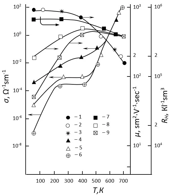
Figure 1. Temperature dependence of the Hall coefficient (curves 1-3), specific electrical conductivity (curves 4-6), and free carrier mobility (curves 7-9) in pure n-InSe crystals with different initial values of their specific resistance in the dark (ρ77):
ρ77, Ω·sm: 1, 4, 7 – 2·103; 2, 5, 8 - 3·105; 3, 6, 9 – 9·106
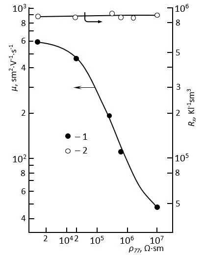
Figure 2. Dependence of the mobility of free primary charge carriers (curve 1) and the Hall coefficient (curve 2) on the initial value of the specific resistance in the dark in pure n-InSe crystals at a temperature of Т=77 K
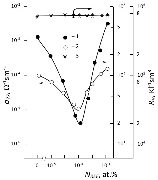
Figure 3. Dependence of the specific electrical conductivity (curve 1), the mobility of free main charge carriers (curve 2), and the Hall coefficient (curve 3) in n-InSe crystals doped with rare earth elements on the amount of dopant added to the sample T=77 K

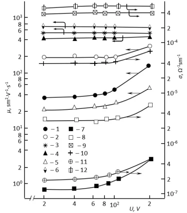
Figure 4. Dependence of the mobility of the main free charge carriers (curves 1-6) and the specific electrical conductivity (curves 7-12) in pure (1-3 and 7-9) and REE-doped (curves 4-6 and 10-12) n-InSe crystals on the intensity of the electric field applied galvanically to the sample
Т = 77 K;
ρ77, Ω·sm: 1, 7 – 9·106; 2, 8 – 3·105; 3, 9 – 2·103
NREE, аt.%: 4, 10 - 10-5; 5, 11 – 5·10-3; 6, 12 - 10-1
The initial, or rather the value of the specific resistance at T=77 K (ρ77) is different for pure, as well as for in samples containing REE additives in the amount of 10-5; 10-4; 5·10-4; 10-3; 5·10-3; 10-2; 5·10-2; 10-1 at.%, the temperature dependence of the specific electrical conductivity (σ), Hall coefficient (RH), mobility of free charge carriers (free electrons) (μ), σ and μ on Е, as well as the dependences of μ, σ, RH on ρ77 and NREE were measured in the range of Т=77÷ 400 K, as well as in the interval from very small values of the intensity of the external electric field (Е) applied galvanically to the sample (corresponding to the linear region of the static current voltage characteristics (CVC) in the dark [33-34]) to the values at which the conversion effect [35] occurs (figure 1-4).
Comparative and statistical analysis of the experimental results (figure 1-4) obtained in experimental measurements showed that in both groups of n-InSe crystal samples taken as the object of study (pure and REE-doped samples) at high (Т>250K) temperatures, as well as in low-ohmic (ρ77<5·103 Ω·sm) pure and doped samples with NREE≥5·10-2 аt.%, the temperature dependences and other properties of the kinetic parameters in the entire temperature range considered (Т=77÷ 400 К) satisfactorily obey (conform) to the existing theoretical provisions for the properties of kinetic parameters in quasi-ordered crystalline semiconductors, while in higher-ohmic (ρ77≥104 Ω·sm) pure and doped samples with NREE<5∙10-2 аt.% In samples of doped crystals, the dependences of σ(Т), μ(Т), RH(Т), μ(ρ77), μ(NREE), σ(NREE), σ(E), μ(E) in the temperature range Т£230÷250 К are anomalous in terms of these provisions. Thus, the fact that the Hall coefficient does not depend on temperature and doping, the increase in the value of the specific electrical conductivity (σ) and the mobility of free charge carriers (μ) of the sample with an increase in temperature with an activation nature, the decrease in the value of μ with an increase in the value of the initial specific resistivity of the sample in the dark (ρ77), the non-monotonic nature of the dependences of σ(NREE) and μ(NREE), the characteristics of the influence of the values of ρ77 and NREE on the nature of the dependence of kinetic parameters on various factors cannot be explained only on the basis of the relevant theoretical provisions available for spatially homogeneous crystalline semiconductors. To explain these dependencies and properties, it is also necessary to take into account the presence of random macroscopic defects (RMD) in the studied samples and the formation of drift barriers for free charge carriers inside the sample due to the presence of these defects.
Since the µ(Т) dependence has the observed activation character, the value of the drift barriers (Δεi) formed in the studied samples was determined according to the slope of the graph constructed on the basis of experimental results and it was shown that for different samples at 77K (depending on the value of ρ77 and NREE) this value is ~0.10÷0.20 eV.
The comparative analyses also show that in the case of the studied samples of high-ohmic pure and doped n-InSe crystals with an added impurity content of NREE<5·10-2 аt.%, the σ(Е) and μ(Е) dependences observed in the experiment are not due to the heating of free charge carriers under the influence of the electric field acting on the sample, or rather, to “hot electron effects”.
According to all the signs observed in practice, these dependencies are associated with a change (reduction) in the height of the drift walls under the influence of the “excess charges” [36-37] created by free primary charge carriers injected into the volume of the sample under study from the current contacts under the influence of an external electric field with a value of Uvol>U2-n [33] (due to their partial compensation of the volume charges).
In our opinion, the fact that the kinetic parameters in n-InSe crystals do not depend on the chemical nature of the introduced REE additives, but only on their amount (NREE), is primarily due to the fact that the effect of the addition on these parameters is not due to the fact that the introduced additive creates an intra-center effect in the studied sample, but rather due to the fact that the level of spatial inhomogeneity of the sample changes depending on the amount of the introduced additive (NREE).
It is assumed that REE dopants (atoms), which are well soluble in semiconductors, are easily ionized when introduced into n-InSe crystals, since they have a small electronegativity. Then, these ions are directed under the influence of the internal electric field existing at the RMD and LO matrix boundary inside the crystal and precipitate (collect) on the RMD.
As a result, at small values of NREE, the influence of RMD on the electrophysical parameters of the crystal increases with its increase, analogous to that of highly doped semiconductors [38]. However, with a further increase in NREE, the distance between the volume charge regions (VCR) of neighboring RMD gradually decreases, and finally this distance becomes smaller than the free flight (LF) or diffusion distance (LD) of free charge carriers in the studied sample [14, 15].
At such large values of NREE, the effect of RMD (or spatial inhomogeneity of the studied sample) on the electrophysical parameters in that sample gradually disappears. For this reason, the μ(NREE) and σ(NREE) dependencies in the studied samples have a non-monotonic nature.
Regarding the nature, origin, and causes of RMD in n-InSe crystals, it should be noted that although they can be very diverse, their main reason is that n-InSe crystals have a layered structure (in these crystals, the chemical bond between neighboring natural layers is weak, or rather, Van der Waals in nature, in the direction perpendicular to the (001) plane). Each RMD formed within the crystal is indistinguishable from the main LO matrix in terms of both its chemical composition and crystal structure, except that their specific resistance in the dark is significantly greater than that of the LO main matrix.
As can be seen from the above, within the framework of the proposed model, samples of high-ohmic (HO) n-InSe crystals can be used as a convenient model for studying various physical parameters and characteristics of “semiconductor-semiconductor” type nanocomposites, i.e., consisting of a high-ohmic chaotic (random) semiconductor nanodispersant and a low-ohmic (LO) semiconductor matrix.
To clarify the characteristics of the electrophysical parameters in single crystals of the layered n-InSe semiconductor, it is necessary to describe these crystals as a whole crystalline semiconductor consisting of a low-ohm (LO) matrix with random macroscopic defects (RMD) of high-ohm (HO). The dependence of electrophysical parameters, namely the specific electrical conductivity, Hall coefficient, and free charge carrier mobility in high-ohmic (HO) crystals of the layered n-InSe semiconductor on temperature, doping, and the intensity of the electric field applied galvanically to the sample is due to the adjustment of the degree of spatial inhomogeneity of the sample under study with temperature, introduced dopants, and the "excess charge" created by injected electrons. High-ohmic single crystals of the layered n-InSe semiconductor can be used as a convenient model for studying the electronic properties of spatially inhomogeneous crystalline semiconductors.
1 M.S. Leanenia, E.V. Lutsenko, M.V. Rzheutski et al. Journal of Applied Physics 129 (2021) 243104. https://doi.org/10.1063/5.0051319
2 E.M. Huseynov, T.G. Naghiyev, Adv. Phys. Res. 1(2) (2019) 99-104.
3 M.A. Jafarov, V.M. Salmanov, A.H. Huseynov et al. UNEC J. Eng. Appl. Sci. 3(2) (2023) 54. https://doi.org/10.61640/ujeas.2023.1207
4 S.G. Asadullayeva, R.A. Ahmedov, A.A. Hadieva et al. UNEC J. Eng. Appl. Sci. 3(2) (2023) 66. https://doi.org/10.61640/ujeas.2023.1209
5 E.M. Huseynov, T.G. Naghiyev, Applied Physics A 128(2) (2022) 115. https://doi.org/10.1007/s00339-022-05265-x
6 R.S. Madatov, A.S. Alekperov, N.N. Gadzhieva et al. International Journal of Modern Physics B 33(09) (2019) 1950066. https://doi.org/10.1142/S0217979219500668
7 A.I. Isayev, S.I. Mekhtiyeva, H.I. Mammadova et al. UNEC J. Eng. Appl. Sci. 4(1) (2024) 55. https://doi.org/10.61640/ujeas.2024.0505
8 T.G. Naghiyev, R.M. Rzayev, Modern Physics Letters B 35(31) (2021) 2150469. https://doi.org/10.1142/S0217984921504698
9 S.G. Asadullayeva, N.A. Ismayilova, T.G. Naghiyev, Modern Physics Letters B 37(34) (2023) 2350166. https://doi.org/10.1142/S021798492350166X
10 M.S. Leanenya, E.V. Lutsenko, V.N. Pavlovskii et al. Journal of Applied Spectroscopy 82 (2015) 53. https://doi.org/10.1007/s10812-015-0063-6
11 A.P. Abdullayev, R.M. Rzayev, T.G. Naghiyev et al. International Journal of Modern Physics B 37(28) (2023) 2350248. https://doi.org/10.1142/S021797922350248X
12 I.I. Aliyev, R.M. Rzayev, K.M. Hashimov et al. Modern Physics Letters B 38(25) (2024) 2450232. https://doi.org/10.1142/S0217984924502324
13 N.A. Verdieva, M.B. Jafarov, R.M. Rzayev, T.G. Naghiyev, International Journal of Modern Physics B 38(03) (2024) 2450034. https://doi.org/10.1142/S0217979224500346
14 R.S. Madatov, F.G. Asadov, E.G. Asadov, T.G. Naghiyev. Journal of the Korean Physical Society 74 (2019) 508.
15 K. Seeger, Physics of Semiconductors, Moscow: Mir (1977) 615 p.
16 V.L. Bonch-Bruevich, S.G. Kalashnikov, Physics of Semiconductors, Moscow: Nauka (1990) 685 p.
17 N. Mott, E. Davis, Electronic Processes in Non-Crystalline Substances, Vol. I and Vol. II, Moscow: Mir (1982) 663 p.
18 V. L. Bonch-Bruevich, I.P. Zvyagin, R. Kuiper, A.G. Mironov, R. Enderlein, B. Esser, Electron Theory of Disordered Semiconductors. Moscow: Nauka, Main Editorial Board of Physical and Mathematical Literature (1981) 384 p.
19 M.K. Sheinkman, A.Ya. Shik, FTP 10(2) (1976) 209.
20 N.B. Brandt, Z.D. Kovalyuk, V.A. Kulbachinsky, Physics and Technology of Semiconductors 22(9) (1988) 1657.
21 A.Sh. Abdinov, R.F. Babaeva, R.M. Rzaev, Inorganic Materials 48(8) (2012) 781. https://doi.org/10.1134/S0020168512080018
22 A.Sh. Abdinov, R.F. Babayeva., E.A. Rasulov, 8th Interntional conference on materials science and condensed matter physics, Chisinau (2016) 56.
23 A.Sh. Abdinov, R.F. Babayeva, Inorganic materials 55(8) (2019) 758.
24 S.L. Stoll, E.G. Gillan, A.R. Barron, Chemical Vapor Deposition 2(5) (1996) 182. https://doi.org/10.1002/cvde.19960020506
25 V. Chikan, D.F. Kelley, Nano Lett. 2(2) (2002) 141. https://doi.org/10.1021/nl015641m
26 U.K. Gautam, S.R.C. Vivekchand, A. Govindaraj, G.U. Kulkarni, N.R. Selvi, C.N.R. Rao, Journal of the American Chemical Society 127(11) (2005) 3658. https://doi.org/10.1021/ja042294k
27 H. Peng, S. Meister, C.K. Chan, X.F. Zhang, Y. Cui, Nano Letters 7(1) (2007) 199. https://doi.org/10.1021/nl062047
28 D.J. Late, B. Liu, H.S.S.R. Matte, C.N.R. Rao, V.P. Dravid, Advanced Functional Materials 22(9) (2012) 1894. https://doi.org/10.1002/adfm.201102913
29 D.V. Rybkovskiy, I.V. Vorobyev, A.V. Osadchy, E.D. Obraztsova, Journal of Nanoelectronics and Optoelectronics 7(1) (2012) 65. http://dx.doi.org/10.1166/jno.2012.1218
30 D.V. Rybkovskiy, A.V. Osadchy, and E.D. Obraztsova, Journal of Nanoelectronics and Optoelectronics 8(1) (2013) 110. https://doi.org/10.1166/jno.2013.1430
31 Z.S. Medvedeva. Chalcogenides of elements of a subgroup of the periodic table, M. Nauka (1968) 216 p.
32 N.F. Kovtanyuk, Yu.A. Kontsevoy Measurements of parameters of semiconductor materials, M. Metallurgy (1970) 429 p.
33 M. Lampert, P. Mark, Injection currents in solids, M. Mir (1973) 416 p.
34 G.A. Akhundov, A.Sh. Abdinov, N.M. Mekhtiev, A.G. Kyazym-zade, FTP 8(11) (1974) 2283.
35 E. Conwell, Kinetic Properties of Semiconductors in Strong Electric Field, М. Мir (1970) 384.
36 A.Sh. Аbdinov, R.F. Babayeva, Journal of Physics: Conference Series (2019) 066047. https://doi.org/10.1088/1742-6596/1400/6/066047
37 S.M. Ryvkin, Photoelectric Phenomena in Semiconductors, Moscow: Nauka (1963) 494 p.
38 B.I. Shklovsky, A.L. Efros Electronic Properties of Doped Semiconductors Moscow: Nauka (1979) 416 p.
A.Sh. Abdinov, R.F. Babayeva, S.I. Amirova, N.A. Rahimova, E.A. Rasulov, Study of the properties of electro-physical parameters in spatially incoherent crystal semiconductors on the example of layered AIIIBVI semiconductor compound crystals, UNEC J. Eng. Appl. Sci. 5(1) (2025) 55-62. https://doi.org/10.61640/ujeas.2025.0506
Anyone you share the following link with will be able to read this content:
This article is licensed under the Creative Commons Attribution ( CC BY 4.0 ) License, which permits unrestricted use, distribution, and reproduction in any medium, provided the original author and source are credited.


M.S. Leanenia, E.V. Lutsenko, M.V. Rzheutski et al. Journal of Applied Physics 129 (2021) 243104. https://doi.org/10.1063/5.0051319
E.M. Huseynov, T.G. Naghiyev, Adv. Phys. Res. 1(2) (2019) 99-104.
M.A. Jafarov, V.M. Salmanov, A.H. Huseynov et al. UNEC J. Eng. Appl. Sci. 3(2) (2023) 54. https://doi.org/10.61640/ujeas.2023.1207
S.G. Asadullayeva, R.A. Ahmedov, A.A. Hadieva et al. UNEC J. Eng. Appl. Sci. 3(2) (2023) 66. https://doi.org/10.61640/ujeas.2023.1209
E.M. Huseynov, T.G. Naghiyev, Applied Physics A 128(2) (2022) 115. https://doi.org/10.1007/s00339-022-05265-x
R.S. Madatov, A.S. Alekperov, N.N. Gadzhieva et al. International Journal of Modern Physics B 33(09) (2019) 1950066. https://doi.org/10.1142/S0217979219500668
A.I. Isayev, S.I. Mekhtiyeva, H.I. Mammadova et al. UNEC J. Eng. Appl. Sci. 4(1) (2024) 55. https://doi.org/10.61640/ujeas.2024.0505
T.G. Naghiyev, R.M. Rzayev, Modern Physics Letters B 35(31) (2021) 2150469. https://doi.org/10.1142/S0217984921504698
S.G. Asadullayeva, N.A. Ismayilova, T.G. Naghiyev, Modern Physics Letters B 37(34) (2023) 2350166. https://doi.org/10.1142/S021798492350166X
M.S. Leanenya, E.V. Lutsenko, V.N. Pavlovskii et al. Journal of Applied Spectroscopy 82 (2015) 53. https://doi.org/10.1007/s10812-015-0063-6
A.P. Abdullayev, R.M. Rzayev, T.G. Naghiyev et al. International Journal of Modern Physics B 37(28) (2023) 2350248. https://doi.org/10.1142/S021797922350248X
I.I. Aliyev, R.M. Rzayev, K.M. Hashimov et al. Modern Physics Letters B 38(25) (2024) 2450232. https://doi.org/10.1142/S0217984924502324
N.A. Verdieva, M.B. Jafarov, R.M. Rzayev, T.G. Naghiyev, International Journal of Modern Physics B 38(03) (2024) 2450034. https://doi.org/10.1142/S0217979224500346
R.S. Madatov, F.G. Asadov, E.G. Asadov, T.G. Naghiyev. Journal of the Korean Physical Society 74 (2019) 508.
K. Seeger, Physics of Semiconductors, Moscow: Mir (1977) 615 p.
V.L. Bonch-Bruevich, S.G. Kalashnikov, Physics of Semiconductors, Moscow: Nauka (1990) 685 p.
N. Mott, E. Davis, Electronic Processes in Non-Crystalline Substances, Vol. I and Vol. II, Moscow: Mir (1982) 663 p.
V. L. Bonch-Bruevich, I.P. Zvyagin, R. Kuiper, A.G. Mironov, R. Enderlein, B. Esser, Electron Theory of Disordered Semiconductors. Moscow: Nauka, Main Editorial Board of Physical and Mathematical Literature (1981) 384 p.
M.K. Sheinkman, A.Ya. Shik, FTP 10(2) (1976) 209.
N.B. Brandt, Z.D. Kovalyuk, V.A. Kulbachinsky, Physics and Technology of Semiconductors 22(9) (1988) 1657.
A.Sh. Abdinov, R.F. Babaeva, R.M. Rzaev, Inorganic Materials 48(8) (2012) 781. https://doi.org/10.1134/S0020168512080018
A.Sh. Abdinov, R.F. Babayeva., E.A. Rasulov, 8th Interntional conference on materials science and condensed matter physics, Chisinau (2016) 56.
A.Sh. Abdinov, R.F. Babayeva, Inorganic materials 55(8) (2019) 758.
S.L. Stoll, E.G. Gillan, A.R. Barron, Chemical Vapor Deposition 2(5) (1996) 182. https://doi.org/10.1002/cvde.19960020506
V. Chikan, D.F. Kelley, Nano Lett. 2(2) (2002) 141. https://doi.org/10.1021/nl015641m
U.K. Gautam, S.R.C. Vivekchand, A. Govindaraj, G.U. Kulkarni, N.R. Selvi, C.N.R. Rao, Journal of the American Chemical Society 127(11) (2005) 3658. https://doi.org/10.1021/ja042294k
H. Peng, S. Meister, C.K. Chan, X.F. Zhang, Y. Cui, Nano Letters 7(1) (2007) 199. https://doi.org/10.1021/nl062047
D.J. Late, B. Liu, H.S.S.R. Matte, C.N.R. Rao, V.P. Dravid, Advanced Functional Materials 22(9) (2012) 1894. https://doi.org/10.1002/adfm.201102913
D.V. Rybkovskiy, I.V. Vorobyev, A.V. Osadchy, E.D. Obraztsova, Journal of Nanoelectronics and Optoelectronics 7(1) (2012) 65. http://dx.doi.org/10.1166/jno.2012.1218
D.V. Rybkovskiy, A.V. Osadchy, and E.D. Obraztsova, Journal of Nanoelectronics and Optoelectronics 8(1) (2013) 110. https://doi.org/10.1166/jno.2013.1430
Z.S. Medvedeva. Chalcogenides of elements of a subgroup of the periodic table, M. Nauka (1968) 216 p.
N.F. Kovtanyuk, Yu.A. Kontsevoy Measurements of parameters of semiconductor materials, M. Metallurgy (1970) 429 p.
M. Lampert, P. Mark, Injection currents in solids, M. Mir (1973) 416 p.
G.A. Akhundov, A.Sh. Abdinov, N.M. Mekhtiev, A.G. Kyazym-zade, FTP 8(11) (1974) 2283.
E. Conwell, Kinetic Properties of Semiconductors in Strong Electric Field, М. Мir (1970) 384.
A.Sh. Аbdinov, R.F. Babayeva, Journal of Physics: Conference Series (2019) 066047. https://doi.org/10.1088/1742-6596/1400/6/066047
S.M. Ryvkin, Photoelectric Phenomena in Semiconductors, Moscow: Nauka (1963) 494 p.
B.I. Shklovsky, A.L. Efros Electronic Properties of Doped Semiconductors Moscow: Nauka (1979) 416 p.