UNEC Journal of Engineering and Applied Sciences Volume 3, No 2, pages 76-85 (2023) Cite this article, ![]() 1195 https://doi.org/10.61640/ujeas.2023.1211
1195 https://doi.org/10.61640/ujeas.2023.1211
Nowadays technology of micro-electrochemical systems is one of the most advanced lines of microware product development. The most salient requirements that can be placed upon the modern and promising products of microware technique is the increase of their function, working frequency and integration level simultaneously with reducing their weight, volume, power consumption and value. To improve characteristics, increase reproducibility and stability of semiconductive barrier structure parameters that are the base of active elements of micro – and nanoelectronics are the most principle applied problems of solid electronics.
In particular, the study of so – called two – dimensional materials as crystalline films of several atoms in thickness which properties can be sharply differed from three – dimensional ones are vigorously proceeding. As for now the most familiar two – dimensional material is graphene having wide perspectives for using in electronic devices. However, graphene is the conductor but both semiconductors and dielectrics are called for in electronic devices. To develop microware devices and elements of nonvolatile memory on the base of metal – dielectric – semiconductor (MDS) the diamond films as a dielectric are used [1, 2].
Diamond is the unique material having a set of unexcelled characteristics. Among other things there have been noted superior diamond properties comparing with other semiconductors: big band gap, high charge carrier mobility and their small lifetime, very big dark resistance and high electric strength, high thermal conductivity as well as the low level of intrinsic noise and high speed of response, elevated temperature and radiation resistance, high chemical stability allowing the diamond devices under unfavorable conditions to be operated [3,4]. Chemical inertness of diamond makes it possible to provide for such coatings deposited from gas phase the additional control by functioning in corrosive medium. Graphene diamond film can be used in nanoelectronics. If the crystal structure is doped by various atoms (for instance, boron, phosphorus and etc.) it displays different type of conductivity. It may be very strong and flexible protection for any surfaces. Due to the high values of breakdown voltage and thermal conductivity it can be applied as an insulator and heat abstraction in high – current and high – voltage electronics. Unique set of physical properties undoubtedly leads to its widespread use in power – engineering, microelectronics, and other fields of young technology [5-9].
Strength and hardness of diamond is related to the high density of carbon atoms in the lattice and strong covalent bonds among them. High thermal conductivity is due to extremely strong interatomic bond, light mass of carbon and simple structure of its crystal lattice with weak anharmonicity. At the expense of record thermal conductivity, the diamond is the best material for different kinds of heat abstraction [10,11], used successfully as a passive element of electronics. For instance, there have been long used discrete heat abstractions for semiconductive devices: avalanche, laser, and Gunn diodes.
Despiterather long-lasting period of investigations the devices with the native diamond do not receive wide acceptance. There is a problem when there aren't two similar crystals, therefore the properties of each device like this is unique that is not advantageous for production type and devices with native diamond are not profitable. Therefore, it is extremely important to use scientists diamond in production. To use exactly the synthetic diamond in production the synthetic seeks to obtain the diamond with necessary and sufficient properties.
Synthetic single crystal grown in high pressure and high temperature (HPHT method) apparatuses have no high quality as native diamonds yet. Therefore, they are not widespread for manufacturing devices on their base. At present the only method to obtain synthetic single crystal diamond layers of high-quality replicating from crystal to crystal is the method of chemical vapor deposition (CVD) in plasma-chemical reactors with carbon – containing gas activation by microwave discharge plasma [12]. Improvement of diamond CVD technology brings about reducing the value of diamond growth and extends capabilities of its usage. The weak point of given method to grow diamond film is a rather low rate of film growth (1-2 μm/h).
Thermodynamic restriction in CVD method gets by with using the process to participate reagents with high chemical potential. Atomic hydrogen sometimes oxygen usually act as an active reagent, are used though it is unjustified to use other active chemical reagents. Atomic hydrogen (H) of high chemical potential is formed during the thermal or plasma activation of reagents. It is involved in several reactions, each of them is thermodynamically efficient and is attended by decreasing Gibbs free energy. These processes form the diamond and atomic hydrogen (H) either participates in hydrocarbon formation or regains molecular form (H²) with the generation of energy obtained from plasma or hot cathode.
Films are applied on the single cryptal silicon substrate by CVD method. Given method allows the parameters of film formation process to be effectively controlled, namely: residual pressure within 0,8÷1,33 Pa (6•10^-3÷10^-4 mm Hg); substrate temperature within 500÷900°C; gas discharge radiation power within 50÷300 W to be varied;various gas and liquid reaction medium to be used. Film formation technology on the substrate is carried out by decomposition in microwave discharge of  gas mixture at the concentration 2%
  – 98%
– 98%  and residual pressure ~0,27 Pa with subsequent deposition of diamond – like layer at high temperature of the substrate [13, 14].
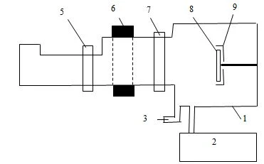
In figure 1 there has been schematized the installation to obtain diamond-like films (DF) in low pressure gas discharge plasma including reaction chamber – 1, system of vacuum pumping – 2, gas system of reaction mixture feed -3, magnetron – 4, circulator – 5, solenoid – 6, dielectric window –7, being transparent for passing the microwave magnetron radiation. In vacuum reaction chamber – 1 being as a cylinder there has been established heated substrate holder – 9 with the substrate -8, which can be transferred along the reaction chamber axis. The temperature of substrate -8 is controlled with accurate up to 3°C. The vacuum system – 2 provides the residual pressure in reaction chamber no more than ~ 6,7•10^(-3) Pа. The system of reaction mixture feed – 3 allows several types of working medium to besimultaneously used. As a radiation source the magnetron M- 105 operating over the frequency 2.45 GHz with maximum power 300W is employed. The circulator – 5 cancels the reflected wave of magnetron – 4. Gas discharge zone in reaction chamber is at the distance 80 mm from the dielectric window – 7. To stabilize gasdischarge the solenoid – 6 with magnetic field 2.5 Tl is applied [15, 16].
Before the beginning of DF deposition, the pressure installation reaction vacuum chamber -1 (figure 1) reduces to the value ~9∙10^(-3) Pa by vacuum system – 2. In this case substrate – 8 heats up to the given temperature (500÷900°C). Then magnetron – 4 turns on at generator radiation power 200Wand the working gas mixture of composition up to residual pressure within 0,14÷0,4 Pa enters the camera – 1. Under the magnetron radiation effectin camera – 1 microware plasma discharge switches on in which ionization reaction goes of ionization and decomposition of gaseous mixture . Because of plasma - chemical reactions on the substrate single crystal silicon KDB – 12 with the orientation /100/ the diamond – like coating is deposited/ The time of applying diamond – like coating is defined by given magnitude of applied film layer thickness and accounts for 50÷120 min.
Figure 1. Diagram of installation for diamond – like film formation in gas discharge plasma of low pressure: 1) Reaction vacuum chamber; 2) Vacuum pumping system; 3) Entry of working gas feed; 4) microware magnetron; 5) Circulator; 6) Solenoid; 7) Transpa
To control the obtained DF thikness a number of methods have been used. By thickness exceeding 1 mkm the interference method realized in microscope “MII – 4” at wavelength λ=605 nm with absolute error no more than 20 nm is used. Films of nanometric thickness is checked on electron and atomic – force microscopes. Structure of diamond – like films is supervised by diffraction patters and electron diffraction patterns on the installation DRON – 4 and by  -radiation as well.
It has been experimentally established that derived in microwave plasma discharge of diamond – like structure films are formed by gaseous mixture decomposition with the concentration 2% – 98% at residual pressure ~0,27 Pa and substrate T~900°C. X -ray study of obtained DF shows that their structure have cubic diamond components with the preferred orientation [100].
Ion implantation of boron into diamond
Diamond doping holds a central position in semiconductive diamond technology. We choose ion implantation process as a technology of diamond material micro-treatment. Given process is widely used in electronics at doping the semiconductive materials by various impurities. Ion implantations offer the advantage over other methods that is the possibility of introducing controllable dose of doping impurity ions up to solubility limit. Ions of implanted material are raised to ion accelerator up to energy 10-5000 keV and penetrate the sample.
Ion implantation brings about disorder of crystal lattice even to amorphization and subsequent graphitization. Ion implantation into crystal lattice of the material being worked leads to the advent of crystal structure defects. Degree of crystal lattice amorphization and disturbed layer depth depends on the kind of interstitial ions, ion number per unit the surface (dose) and their energy.
Therefore, it is necessary to carry out post-implantation annealing crystals: first, for crystal lattice reduction, second, for electric activation of impurity interstitial atoms. While heating the crystal lattice is regained, the epitaxial growth of solid phase on the base of crystal lattice arranged deeper than the region disturbed by ions is taken place.
The issue of diamond doping is concerned with the high concentration of carbon atoms in the lattice being the highest among all the semiconductors, high energy of atomic bonds and their small atomic radius. So, the number of impurities capable of isomorphous substitution of carbon atoms in diamond crystal lattice is rather limited. As doping atoms for diamond, the boron, nitrogen, and phosphorus are best suited to the radius relation. Phosphorus atoms substituting the carbon in lattice sites have very small solubility in diamond. Nitrogen is the donor with deep centers.
Nowadays the main method of doping native diamond is the boron ion implantation of boron – acceptor impurity giving rise shallow levels with the activation energy Ea=Ev+0.37eV. As a practical matter of special interest is the space distribution of boron atoms introduced by ion implantation in diamond. The calculation of space distribution of implanted boron atoms is made out by SRIM-2013 (Stopping Range InMaterial) [17].
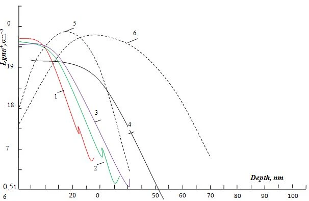
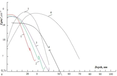
In Figure 2 there have been presented distributions in depth of boron atoms introduced into the diamond with different energy (E=10-25 keV) through the aluminum screen 30-80 nm in thickness (curves 1-4) and no screen (curves 5-6). Aluminum screen thickness for corresponding boron ion energy is chosen so that the projective range of boron ions in Al is at the interphase of screen – diamond. From Figure 1 it is seen that in the case of Al screen presence the profile maximum of boron atom distribution lies along the near-surface layer 12-20 nm in thickness (curves 1-4) but the “tail” of the profile (maximum range of boron ions) extends down to 30-50 nm in depth.
B^+ ion implantation in uncoated diamond (curves 5-6) tends to the fact that boron atomconcentration 10 nm in depth in near -surface layer is by the order of 2 lower than in neighborhood of projective range that does not enable the surface δ- doped p-channel without etching the surface at a depth of 20-30 nm to be created.
Nitrogen is the deep donor center in diamond with the energy activation 1.7 eV and consequently its contribution to the electro-conductivity is negligibly small. As it is seen from Figure 2 in near -surface at a depth of 10 nm the concentration of interstitial nitrogen atoms with energy 15-20 keV is by the order lower than the concentration of boron atoms (curves 1-4) and hence in this region boron is not overcompensated by nitrogen and δ- doped p-channelby boron is formed. In profile tail region of boron atom distribution, the nitrogen concentration exceeds the boron concentration. Thus, nitrogen donor centers compensate boron acceptor centers and given region has a resistance which is in excess of p-channel resistance by the order of several magnitudes [18].
Figure 2. Depth distribution of boron atoms embedded in diamond with different energies through an Al mask and without a mask. Аl mask thickness, enerji of В+: 1-Al-30nm, 10кеV, 2-Al-50nm, 15кеV, 3-Al-70nm, 20кеV, 4-Al-80nm, 25кеV, 5-without a mask, 10ке
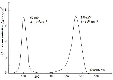
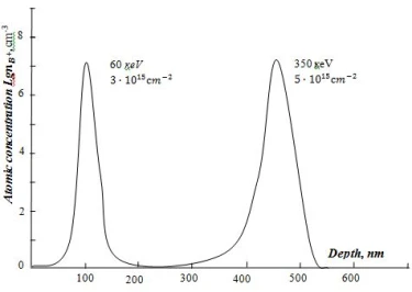
In Figure 3 shows the distribution profiles of implanted boron atoms upon implantation with energies of 60 and 350 keV with doses of 3⋅10^15 and 5⋅10^15 cm¯², respectively. As it is seen from figure the boron ion implantation with high energy E=350 keV makes possible to create hidden conducting layers but low energy implantation creates near surface conducting layers. In case of B^+ ion implantation at high energy (E=350 keV) the post-implantation annealing generates the conducting buried layer 100nm in thickness. By boron ion energy 2 MeV the conducting buried layers are formed at a depth of 1.2 mkm. When choosing boron ion dose and energy one can produce buried highly compensated, weakly doped layers of p- type and highly doped conducting layers of p^+-type.
Figure 3. Distribution of boron atoms in a diamond crystal under different implantation modes
Given buried layer can be used as a channel of MIS- transistor. In this case as a dielectric there has been served diamond non-conducting near–surface layer 200 nm in thickness that mounts metal gate according to standard technology. The realizability of the technology like this is due to the fact that diamond has a very big resistivity 10^12÷10^13 Оhm∙сm, then the current leak through the diamond gate dielectric is insignificant.
Diamond CVD films have surface conductivity disappearing after annealing in the air or treatment in oxidizing acids. p-type conductivity generates after the diamond treatment in hydrogen plasma causes the formation of С–Н bonds on crystal surface [19]. The resistance of the hydrogenated surface immediately after plasma treatment is quite high, ~10^10 Оhm⁄сm , but in air it drops down to,~10^4 Оhm⁄сm^2 [20]. Thus conductivity is related to atmospheric gas absorption which is hydrogenated by the diamond surface. Recently it is shown that NO2 and O3 gas addition in the air can increase surface conductivity by several fold.
This paper deals with the diamond plates synthetic CVD single crystals [22]. Transverse size of plates is 3-3.5 mm, thickness is 0.3-0.5 mm.
Crystallographic orientation of surface is (100). Plate surface undergoes the mechanical polish to the roughness ˂ 5 nm. To form the hydrogenated surface the crystals are annealed in hydrogen at atmospheric pressure. After cooling in hydrogen atmosphere, the crystals are placed in the air and they acquire conducting properties.
It is established that as a result of annealing in hydrogen at atmospheric pressure for 30 min, the layer formation occurs when temperatures reach above 700°C with p-type conductivity on diamond hydrogenated surface. The best results (mobility 150-200 сm^2⁄((V∙с))) were obtained by heat treatment of (100) CVD diamond layers in a hydrogen flow in the temperature range 800-1000°C. At a temperature of 700°C, the conductive layer apparently just begins to form, so it has a high resistance. Given method of thermal treatment in hydrogen can be an alternative to the conventional method of H-layer formation in microwave hydrogen plasma as a simpler and more reproducible [23, 24].
Electrophysical properties of diamond
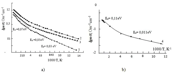
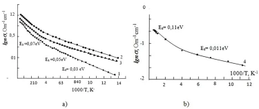
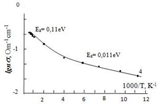
The Van der Pauw method was used to study the temperature dependence of the specific conductivity DF after implantation of different energies of boron ions (1-10 kV, 2-15 kV, 3-20 kV, 4-20 kV) in the temperature range 80–700 K. Results of dependence σ(T) for all four crystals are presented in figure 4. Samples 1-3 are measured by the initial surface, the fourth crystal doped surface is partially etched. Samples 1-3 have close conductivity values. It is seen that on dependence σ(T) three portions of different low activation energy varyingat low temperatures from  up to
up to  at high temperatures have been obviously observed. Similar dependence of conductivity on the temperature with low activation energy Ea=0.05-0.11 eV is evident in polycrystalline CVD diamond implanted by boron with high energy 60 keV and high dose 2∙10^16 cm^2 (figure 4)[25].
The authors of [26] associate the increase in activation energy with increasing temperature with the blurring of the acceptor level of boron in the doped layer due to the inhomogeneity of the depth distribution of boron atoms, which is caused by the overlap of the ranges of B^+ ions at different energies. In areas with higher boron concentrations, the Ea level is shallower, and in areas with lower boron concentrations, it is deeper [27]. Therefore, at low temperatures, boron first begins to be activated from shallower levels, and with increasing temperature, the concentration of electrically active boron and, consequently, conductivity, increases due to deeper centers. This is confirmed by the temperature dependence of conductivity for sample 4 with partially etched by doped layer which is by two orders of magnitude lower than the conductivity for samples 1-3 (figure 4). Lesser conductivity of etched layer is due to the boron distribution in tail of range with lower concentration and hence at high temperatures the activation energy of given sample  is much higher than non-etched samples ( ) [28].
Figure 4. Dependences of diamond specific conductivity doped by boron under B+ ion polyenergetic implantation on the temperature of measured initial samples (a) 1-10 kV, 2-15 kV, 3-20 kV and sample etchedpartially by surface (b) 4-20 kV
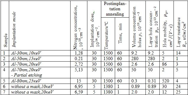
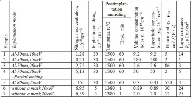
Hall measurementsresults of implanted electrophysical parameters in the second experiment is given in table. It is seen from the Table that the hole concentration and mobility slightly go from implantation and annealing regimes. However, nitrogen concentration has a profound effect on electrophysical parameters. Due to the nitrogen high concentration in native diamond, it is difficult to judge the efficiency of boron interstitial atom activation and to determine the compensation degree as the boron can be involved in neutral donor-acceptor complexes [29]. Sample 2 (table) has the lowest nitrogen concentration and the biggest hole concentration. On the contrary, sample 5 (table) has the highest nitrogen concentration and the lowest hole concentration. In this sample the strong compensation of electrically active boron by nitrogen donor centers has been taken place. Because of low hole concentration in sample 5 their mobility (520 cm²/(V⋅c)) comparing with other crystals is substantially increased. The record hole mobility 1150 cm²/(V⋅c) at layer concentration, an order magnitude lower than for sample 5) has been obtained in paper [25], CVD diamond films implanted by boron and annealed under the conditions which are analogous with ones that are mentioned in table.
Thus, ion implantation of boron large doses allows the conducting layers with high hole mobility and high conductivity even at room temperature to be obtained that is due to the low activation energy of implanted boron at high concentration.
The conductivity of hydrogenated diamond is superficial since it disappears even after short-term (~1 min or less) treatment in air plasma at a pressure of 0.5 Torr at which etching of the crystal does not occur. At the same time, the surface is stable in air up to a temperature of 300°C at higher temperatures, the conductivity begins to slowly decrease.
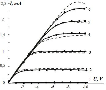
The possibility of field effect transistor based on the obtained material.
Sequence of technological operation production of field-effect transistor on hydrogenated diamond is given in [30,31]. After mechanical polishing of the surface, the crystal was annealed in a hydrogen atmosphere at a temperature of 900°C for 20 min to form a hydrogenated surface. Then a layer about 200 nm thick was deposited on the entire surface of the crystal using resistive evaporation in a vacuum. Thereafter by photolithography the metal is etched beyond the active zone of transistor. And to isolate active zone the sample has been completed in air plasma at pressure 0.4 Torr for 1 min that eliminates the hydrogen surface on open sections but holds it in active zone safeguard with Cu layer. On pre-treated sample like this the screen of photoresist with gate window. Next Cu etching has been carried out under the gate by etching under the resist edge to provide the clearance between the contacts of gate and source-drain. By method of resistive evaporation in vacuum there has been deposited Cu layer 60 nm in thickness on the sample after which the resist is removed. For measurements we connect the wire with silver contact adhesive (“Contactol”). Length of gate L=35mkm, width W=1 mm, clearance between source-gate and gate-source is about 75 mkm. In Figure 5 shows the volt-ampere characteristics (VAC) of the manufactured sample. In the drain–source voltage range of 0–10 V and gate–source voltage of 0–5 V, the fabricated sample demonstrated the basic properties of field-effect transistors, namely: current modulation by gate voltage, channel overlap, and saturation [16]. This sample demonstrates low gate leakage, namely low current at zero drain voltage and no VAC slope in saturation mode.
Figure 5. Volt-ampere characteristic of a transistor made on a hydrogenated surface of a diamond sample (solid lines - experimental, dashed lines - calculation using a smooth channel model), Vзи=0 (1), -1(2), -2(3), -3(4), -4(5), -5V(6)

Above-mentioned volt-ampere characteristics can be well described by fair channel model where the contact and conducting channel are represented as capacitor plates with the surface capacity-voltage characteristics in [18] the mobility is equal to μ = 70 cm²/(V⋅c).
If the barrier layer has a structure with dielectric constant ἐ=5.7 the specific capacity 1 mF/cm2 is in agreement with the layer 5 nm in thickness. Maximum gate voltage when the measurements are carried out U=5V . After voltage dropresidue at the gap source-gate the potential differentiation between gate contact and conducting channel the source side is equal to 1.6 V. Thus, within given model the intensity in dielectric barrier in this regime is 30 MV/cm that even exceeds the theoretical intensity of diamond breakdown (this calculation does not correct surface potential of diamond). Indeed, after gate voltage feed U=-7V ( in other samples of transistor the results of previous measurements failed to be reproduced: subsequent measurements display large leakage through the gate as evidences the breakdown.
As a result of investigating processes of native diamond doping by boron ion implantation method it is revealed that given method allows the conducting layers with high hole mobility and high conductivity at room temperature to be obtained. Homoepitaxial diamond structures grown by chemical vapor deposition (CVD) in hydrogen plasma have high electrophysical parameters indicating high perfection of material. It is good for manufacturing semiconductive devices on its base, which are in operation over a wide temperature range.
In uncoated diamond, boron implantation leads to the fact that in the near-surface layer the concentration of boron atoms is almost two orders of magnitude lower than in the vicinity of the projected path, which does not allow the creation of a surface p-channel.
In the temperature dependence of the electrical conductivity of the implanted diamond, three regions with different low activation energies are observed, which varies from at low temperatures to  at high temperatures. The increase in activation energy with increasing temperature is associated with the blurring of the acceptor level of boron in the doped layer due to the heterogeneity of the distribution of boron atoms in depth. At low temperatures, boron first begins to be activated from shallower levels, and with increasing temperature, the concentration of electrically active boron and, consequently, conductivity, increases due to deeper centers.
Ion implantation of large doses of boron ions makes it possible to obtain conductive layers with high conductivity already at room temperature, which is due to the low activation energy of implanted boron at high concentrations.
The possibility of creating a field-effect transistor on a hydrogenated diamond surface with a maximum gate voltage of 5 V has been demonstrated.
1 M.H. Nazare, A.J. Neves, Properties, Growth and Application of Diamond, The Institution of Electrical Engineers (2001) 427p.
2 C.J.H. Wort, R.S. Balmer, Materials Today 11(1-2) (2008) 22. https://doi.org/10.1016/S1369-7021(07)70349-8
3 A. Raveendran, M.T. Sebastian, S. Raman, Journal of Electronic Materials 48(5) (2019) 2601. http://dx.doi.org/10.1007/s11664-019-07049-1
4 T. Clarkson, Materials Science and Technology 38(16) (2022) 1332. https://doi.org/10.1080/02670836.2022.2073946
5 T. Iwasaki, H. Kato, T. Makinoet, M. Ogura, D. Takeuchi, S. Yamasaki, M. Hatano, IEEE Journal of the Electron Devices Society 5(1) (2017) 95. http://dx.doi.org/10.1109/JEDS.2016.2624301
6 T. Matsumoto, H. Kato, T. Makino, M. Ogura, D. Takeuchi, S. Yamasaki, M. Imura, A. Ueda, T. Inokuma, N. Tokuda, Japanese Journal of Applied Physics 57(4S) (2018) 04FR01. https://doi.org/10.7567/JJAP.57.04FR01
7 S. Li, Y. Wang, M. Yang, J. Miao, K. Lin, Q. Li, X. Chen, J. Deng, X. Xing, Mater. Adv. 3(14) (2022) 5735. https://doi.org/10.1039/D2MA00381C
8 S. Zhang, B. Malič, J.-F. Li , J. Rödel, Journal of Materials Research 36 (2021) 985. https://doi.org/10.1557/s43578-021-00180-y
9 L. Pierantoni, D. Mencarelli, IEEE Nanotechnology Magazine 15(5) (2021) 7. https://doi.org/10.1109/MNANO.2021.3097490
10 V. Ralchenko, V. Konov, Journal "Electronics: Science, Technology, Business" 4 (2007) 58.
11 T. Clarkson, Materials Science and Technology 38(16) (2022) 1332.
12 R.A. Khmelnitsky, N.Kh. Talipov, G.V. Chucheva, Synthetic diamond for optics M., Iz.IKAR (2017) 228p
13 D. Bennett, M.M. Basagoiti, E.Artacho, R Soc Open Sci. 7(11) (2020) 201270. https://doi.org/10.1098/rsos.201270
14 M.S.Afanasyev, P.A.Luchnikov, A.Yu.Mityagin, G.V.Chucheva, Bulletin of Science of Siberia Series 5 1(2) (2012) 114.
15 I. Castillo, K.K. Mishra, R. Katiyar, Crystals 13(4) (2023) 630. https://doi.org/10.3390/cryst13040630
16 N. Zhang, D. Wang, J. Wang, H. Fang, B. He, J. Guo, Y. Han, P. Zhang, C. Shi, Y. Chen, Q. Wang, M. Ren, W. Lü, Coatings 11(12) (2021) 1491. https://doi.org/10.3390/coatings11121491
17 J.F. Ziegler, The Stopping and Range of Ions in Matter. http://www.srim.org
18 V. Kavitha, P. Mahalingam, M. Jeyanthinath, N. Sethupathi, Mater. Today Proc. 23(12-5) (2020).
19 H. Kawarada, Surface Sci. Reports 26(7) (1996) 205. https://doi.org/10.1016/S0167-5729(97)80002-7
20 J. Ristein, F. Maier, M. Riedel, M. Stammer, Diamond and Related Mater 10(3) (2001) 416. http://dx.doi.org/10.1016/S0925-9635(00)00555-0
21 H. Sato, M. Kasu, Diamond and Related Mater. 24 (2012) 99. https://doi.org/10.1016/j.diamond.2011.12.004
22 Yu.V. Gulyaev, A.Yu. Mityagin, G.V. Chucheva, M.S. Afanasyev, K.N. Zyablyuk, N.Kh. Talipov, P.G. Nedosekin, A.E. Nabiev, Radioengineering and electronics 59(3) (2014) 304. https://doi.org/10.7868/s0033849414030061
23 H.A. Gatea, I.S. Naji, Journal of Advanced Dielectrics 10(5) (2020) 2050021. https://doi.org/10.1142/S2010135X20500216
24 S. Lahiry, Trends in Sciences 20(6) (2023) 5147. https://doi.org/10.48048/tis.2023.5147
25 A.A. Altukhov, A.L. Vikharev, A.M. Gorbachev, M.P. Dukhnovsky, V.E. Zemlyakov, K.N. Zyabluk, A.V. Mitenkin, A.B. Muchnikov, D.B. Radishchev, A.K. Ratnikova, Yu.Yu. Fedorov, FTS 45(3) (2011) 403.
26 K.N. Zyablyuk, A.Yu. Mityagin, N.Kh. Talipov, Technology and design in electronic equipment 5 (2012) 39.
27 A. Pietrenko-Dabrowska, S. Koziel, A.G. Raef, Electronics 11(24) (2022) 4094. https://doi.org/10.3390/electronics11244094
28 M.S. Afanasiev, E.I. Goldman, G.V. Chucheva, A.E. Nabiev, J.I. Huseynov, and N. Sh. Aliyev, Physics of the Solid State 62(1) (2020) 121.
29 M. Afanasiev, A. Nabiev, G.V. Chucheva and J.I. Huseynov , Key Engineering Materials 781 (2018) 20.
30 A. Hokazono, T. Ishikura, K. Nakamura, S. Yamashita, H. Kawarada, Diamond and Related Mater 6 (1997) 339. https://doi.org/10.1016/S0925-9635(96)00726-1
31 Yu.V. Gulyaev, A.S. Bugaev, A.Yu. Mityagin and et al., Journal Achievements of Modern Radioelectronics 12 (2011) 3.
A.E. Nabiyev, J.I.Huseynov, Growth of synthetic diamond films and their electrophysical properties, UNEC J. Eng. Appl. Sci. 3(2) (2023) 76-85 https://doi.org/10.61640/ujeas.2023.1211
Anyone you share the following link with will be able to read this content:
This article is licensed under the Creative Commons Attribution ( CC BY 4.0 ) License, which permits unrestricted use, distribution, and reproduction in any medium, provided the original author and source are credited.

M.H. Nazare, A.J. Neves, Properties, Growth and Application of Diamond, The Institution of Electrical Engineers (2001) 427p.
C.J.H. Wort, R.S. Balmer, Materials Today 11(1-2) (2008) 22. https://doi.org/10.1016/S1369-7021(07)70349-8
A. Raveendran, M.T. Sebastian, S. Raman, Journal of Electronic Materials 48(5) (2019) 2601. http://dx.doi.org/10.1007/s11664-019-07049-1
T. Clarkson, Materials Science and Technology 38(16) (2022) 1332. https://doi.org/10.1080/02670836.2022.2073946
T. Iwasaki, H. Kato, T. Makinoet, M. Ogura, D. Takeuchi, S. Yamasaki, M. Hatano, IEEE Journal of the Electron Devices Society 5(1) (2017) 95. http://dx.doi.org/10.1109/JEDS.2016.2624301
T. Matsumoto, H. Kato, T. Makino, M. Ogura, D. Takeuchi, S. Yamasaki, M. Imura, A. Ueda, T. Inokuma, N. Tokuda, Japanese Journal of Applied Physics 57(4S) (2018) 04FR01. https://doi.org/10.7567/JJAP.57.04FR01
S. Li, Y. Wang, M. Yang, J. Miao, K. Lin, Q. Li, X. Chen, J. Deng, X. Xing, Mater. Adv. 3(14) (2022) 5735. https://doi.org/10.1039/D2MA00381C
S. Zhang, B. Malič, J.-F. Li , J. Rödel, Journal of Materials Research 36 (2021) 985. https://doi.org/10.1557/s43578-021-00180-y
L. Pierantoni, D. Mencarelli, IEEE Nanotechnology Magazine 15(5) (2021) 7. https://doi.org/10.1109/MNANO.2021.3097490
V. Ralchenko, V. Konov, Journal "Electronics: Science, Technology, Business" 4 (2007) 58.
T. Clarkson, Materials Science and Technology 38(16) (2022) 1332.
R.A. Khmelnitsky, N.Kh. Talipov, G.V. Chucheva, Synthetic diamond for optics M., Iz.IKAR (2017) 228p
D. Bennett, M.M. Basagoiti, E.Artacho, R Soc Open Sci. 7(11) (2020) 201270. https://doi.org/10.1098/rsos.201270
M.S.Afanasyev, P.A.Luchnikov, A.Yu.Mityagin, G.V.Chucheva, Bulletin of Science of Siberia Series 5 1(2) (2012) 114.
I. Castillo, K.K. Mishra, R. Katiyar, Crystals 13(4) (2023) 630. https://doi.org/10.3390/cryst13040630
N. Zhang, D. Wang, J. Wang, H. Fang, B. He, J. Guo, Y. Han, P. Zhang, C. Shi, Y. Chen, Q. Wang, M. Ren, W. Lü, Coatings 11(12) (2021) 1491. https://doi.org/10.3390/coatings11121491
J.F. Ziegler, The Stopping and Range of Ions in Matter. http://www.srim.org
V. Kavitha, P. Mahalingam, M. Jeyanthinath, N. Sethupathi, Mater. Today Proc. 23(12-5) (2020).
H. Kawarada, Surface Sci. Reports 26(7) (1996) 205. https://doi.org/10.1016/S0167-5729(97)80002-7
J. Ristein, F. Maier, M. Riedel, M. Stammer, Diamond and Related Mater 10(3) (2001) 416. http://dx.doi.org/10.1016/S0925-9635(00)00555-0
H. Sato, M. Kasu, Diamond and Related Mater. 24 (2012) 99. https://doi.org/10.1016/j.diamond.2011.12.004
Yu.V. Gulyaev, A.Yu. Mityagin, G.V. Chucheva, M.S. Afanasyev, K.N. Zyablyuk, N.Kh. Talipov, P.G. Nedosekin, A.E. Nabiev, Radioengineering and electronics 59(3) (2014) 304. https://doi.org/10.7868/s0033849414030061
H.A. Gatea, I.S. Naji, Journal of Advanced Dielectrics 10(5) (2020) 2050021. https://doi.org/10.1142/S2010135X20500216
S. Lahiry, Trends in Sciences 20(6) (2023) 5147. https://doi.org/10.48048/tis.2023.5147
A.A. Altukhov, A.L. Vikharev, A.M. Gorbachev, M.P. Dukhnovsky, V.E. Zemlyakov, K.N. Zyabluk, A.V. Mitenkin, A.B. Muchnikov, D.B. Radishchev, A.K. Ratnikova, Yu.Yu. Fedorov, FTS 45(3) (2011) 403.
K.N. Zyablyuk, A.Yu. Mityagin, N.Kh. Talipov, Technology and design in electronic equipment 5 (2012) 39.
A. Pietrenko-Dabrowska, S. Koziel, A.G. Raef, Electronics 11(24) (2022) 4094. https://doi.org/10.3390/electronics11244094
M.S. Afanasiev, E.I. Goldman, G.V. Chucheva, A.E. Nabiev, J.I. Huseynov, and N. Sh. Aliyev, Physics of the Solid State 62(1) (2020) 121.
M. Afanasiev, A. Nabiev, G.V. Chucheva and J.I. Huseynov , Key Engineering Materials 781 (2018) 20.
A. Hokazono, T. Ishikura, K. Nakamura, S. Yamashita, H. Kawarada, Diamond and Related Mater 6 (1997) 339. https://doi.org/10.1016/S0925-9635(96)00726-1
Yu.V. Gulyaev, A.S. Bugaev, A.Yu. Mityagin and et al., Journal Achievements of Modern Radioelectronics 12 (2011) 3.