UNEC Journal of Engineering and Applied Sciences Volume 5, No 2, pages 88-97 (2025) Cite this article, ![]() 528 https://doi.org/10.61640/ujeas.2025.1207
528 https://doi.org/10.61640/ujeas.2025.1207
Currently, an intensive search is underway for new promising semiconductor materials of the AIIIBIIIC2VI type, including semiconductor compounds TlGaS2, of particular interest, the laws of many physical phenomena in which have not received sufficient coverage in the specialized literature, containing several elements that would allow their characteristics and properties to be controlled. TlGaS2, a layered compound of thallium gallium sulfide, belongs to a class of materials known for their unique nonlinear optical properties, high thermal stability, and significant interest in photonic and optoelectronic devices. Due to its layered structure, TlGaS2 exhibits anisotropic properties that make it highly sensitive to external factors such as electron radiation. Exposure to radiation can lead to significant changes in the structure, properties, and surface morphology of the crystal, which can affect its performance in various applications such as radiation sensors, high-energy detectors, and solid-state lasers.
The atomic stack of the crystals consists of two twisted anionic layers with weakly bound Tl1+ cations located in triangular cavities between them. As a result, the crystals consist of individual layers with weak bonds between layers and strong bonds between atoms within layers [1-5].
In general, AIIIBIIIC2VI types of compounds known as high defective, wide band materials [6-10]. Therefore, these materials also have good doping availability in high concentration. Due to these advantages this types of materials have very wide application possibilities in wide range of areas [11-16].
In recent years, layered chalcogenide semiconductors have attracted increasing attention owing to their remarkable structural and optical characteristics. Their inherent crystallographic anisotropy, together with highly tunable physical, in particular, optical properties, makes these materials strong candidates for advanced optoelectronic and photonic technologies [17-20]. Previous studies indicate that TlGaS2 is a wide-band-gap semiconductor active in the visible to near-ultraviolet region, exhibiting strong optical absorption and notable nonlinear optical effects [12-20]. These characteristics make it a promising material for photodetectors, frequency-conversion devices, optical limiters, and radiation sensors. In addition, the presence of heavy thallium atoms enhances spin–orbit interactions, which can significantly affect the electronic structure and enable spin- and polarization-dependent functionalities.
Related layered chalcogenides, including TlInS2, GaS, and InSe, display similar or complementary properties, emphasizing the importance of comparative investigations within this material family [7-10, 20]. However, the relationships between crystal structure and physical properties in TlGaS2-based systems remain insufficiently understood, particularly under varying external conditions such as temperature, pressure, and excitation energy.
Thus, from the above it can be said that TlGaS2 has a strong covalent bond created between the atoms within the layer, while a weak van der Waals bond is formed between the atoms between the layers. Therefore, TlGaS2 crystals can be easily separated into their own monolayers, which makes them quasi-two-dimensional (2D) materials with unique physical properties. The indirect band gap of bulk crystals changes to a direct band gap when they are transformed into a 2D monolayer [21]. The indirect band gap was estimated to be approximately 2.45 eV, while the direct band gap was reported to be approximately 2.55 eV [22]. The conductivity of TlGaS2 crystals was found to be about 10−7 (Ohm cm)-1 at 300 K [23]. TlGaS2 has been reported to exhibit high sensitivity to visible, infrared and X-ray ranges [24]. The monoclinic crystal structure of the TlGaS2 compound contains the space group C2/c and the lattice parameters a = 10.87 Å, b = 10.79 Å, c = 15.70 Å and β = 100.47°, respectively [25]. In works [26, 27] photoconductive, photovoltaic, photoluminescent, thermal expansion, nonlinear optical and Raman characteristics of TlGaS2 crystals were investigated. Thus, due to its attractive physical properties, TlGaS2 is considered as a promising material for optoelectronic devices.
From the above literature data, it is known that the effect of electron irradiation on the structural and surface morphological properties of TlGaS2 single crystals has become a subject of considerable interest due to their potential applications in optoelectronics, laser devices and high-performance electronics. Understanding how electron irradiation affects its structure and surface morphology is crucial for optimizing its use in radiation-sensitive applications.
Therefore, the aim of our study of the effect of electron irradiation on the structural integrity, surface roughness, defect formation and general properties of the material of TlGaS2 single crystals is relevant.
To achieve the set goal, TlGaS2 single crystals were used, synthesized by fusing components in a stoichiometric ratio in evacuated (~10-4 mm rt.st) and sealed quartz ampoules. The following were used as initial components for the synthesis: ultra-pure elements of thallium Tl-00, gallium of the GLV4 brand, elemental sulfur of ultra-pure grade OSI-16-5. To further study the physical properties of solid solutions, large single crystals were grown using the Bridgman-Stockbarger method [27].
Single crystals of TlGaS2 are easily cleaved in two mutually perpendicular directions. Samples for measuring optical properties were prepared from freshly cleaved plane-parallel plates. TlGaS2 single crystal plates cleaved in the cleavage plane are extremely stable in terms of physical parameters during long-term storage and temperature changes. By means of chipping, photosensitive elements of any thickness can be obtained, which do not require grinding and polishing. Therefore, the technique of producing samples from TlGaS2 single crystals is distinguished by its simplicity. The plane-parallel plates obtained by cleaving, for which the optical axis is normal to the surface, had the form of thin plates with a thickness of 10 to 100 µk.
The irradiation of the studied crystal samples with electrons with an energy of 2 MeV and a beam current density of 0.085 μA/cm2 was carried out on the Elektronika U-003 accelerator of the INPUzA. The electron energy was chosen according to the sample’s density and thickness, and it was determined using a standard calibration wedge (P4701) "Riso 2 Piece Aluminum" (Belgium) composed of aluminum [28-31].
A favorable condition for creating various functional devices is obtaining a material with certain parameters, which necessitates a comprehensive study of the presence of inhomogeneities in their structure, composition and properties. The study of crystalline surfaces allows one to control changes in surface properties during spatial transitions during crystal growth, as well as to clarify some physical and chemical properties. Electron probe microanalysis methods are of great importance in monitoring the composition of crystals, nanomaterials and polymers. To obtain three-dimensional images of the surface morphology of single crystals, a modern microscope SPM 9700HT (Shimadzu) was used. The study was conducted in the dynamic scanning mode for viewing the sample under the microscope. The boundaries of the surface of single crystals were chosen with a width of 15 by 15 μm. In the following text the following notations are used: Ra is the arithmetic mean deviation of the profile from the mean line drawn by the least square’s method within the base length, Rz is the height of the profile irregularities at 10 points, i.e., the average value of the absolute heights of the five largest profile protrusions and the depth of five depressions along the greatest length of the profile. Base length is the length of the line used to highlight irregularities characterizing the surface roughness and quantitatively assess its parameters.
The results of X-ray diffraction studies of the obtained crystals were studied. First of all, the quality of the single crystal was determined. Using X-ray diffraction patterns, the spatial position of the crystals, the symmetry of the syngony regions and the suitability of the crystals for X-ray diffraction methods were determined. A copper tube was used to determine the parameters of the elementary lattice of the crystals using X-rays and to obtain information on the structure of atoms and molecules. X-ray diffraction data were recorded using a Malvern Pananalytical Empyrean analytical diffractometer with CuKα radiation (λ = 1.54 Å). In this experiment, the high-voltage generator is 10-60 kV; current 10-60 mA; The maximum used angular range of the Bragg-Brentano beam with a power of 4 kW is 2θ = 10° ÷ 100°. The X-ray diffraction scanning speed is assumed to be 0.3 deg/min. The X-ray structural analysis data were processed using the Rietveld method using the FullProf program [32-35].
Based on the obtained X-ray powder diffraction data, the crystallite size was determined using the Debye-Scherrer formula [36-40]:
 (1)
(1)
where D is the average crystallite size, K is the geometric coefficient (0.9), λ is the X-ray wavelength (1.5406 Å), β is the full width of the diffraction reflection at half maximum (FWHM), θ is the diffraction angle.
The dislocation density was determined by the equation [41,42]:
 (2)
(2)
The value of microstresses in the TlGaS2 crystal was calculated using the Stokes-Wilson equation:
 (3)
(3)
Processing of the X-ray diffraction pattern (figure 1) showed that the initial TlGaS2 single crystal has a monoclinic (sp.gr. C2/c) structure. The unit cell parameters are a = 10 Å, b = 10 Å, c = 14.973 Å.
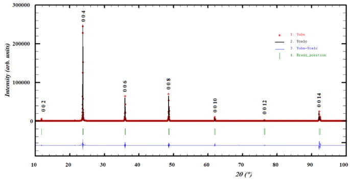
Figure 1. X-ray diffraction pattern of a TlGaS2 single crystal: I – experimental and calculated data; II – Bragg reflections; III – difference curve between experimental and calculated data
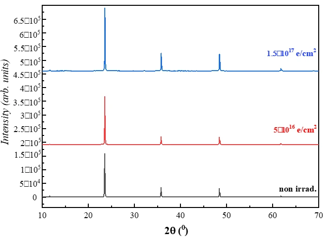
Figure 2 shows the analysis of general X-ray diffraction spectra in the range of 10° - 70° on the dependence of the irradiation dose. Comparing three cases: unirradiated sample - black spectrum, irradiated with a dose of 5×10¹⁶ e/cm² - red spectrum and a sample irradiated with a dose of 1.5×10¹⁷ e/cm² - blue spectrum.
Comparative results show that the intensity of the peaks increased with increasing radiation dose. This may indicate a change in X-ray transparency or a more ordered crystal lattice. At high doses, recrystallization or rearrangement of the single crystal structure is possible.
The main results of the above study show that with increasing radiation dose, the intensity peaks shift from 23.54 to 23.6 towards a larger angle (figure 3). The physical mechanisms of this result are explained by the presence of compressive stresses in the crystal lattice, since electron beam irradiation can create dislocations and defects that lead to a decrease in the lattice parameter. The results of the structural characteristics of the TlGaS2 single crystal irradiated with accelerated electrons are given in table 1 and reflected in figure 4.
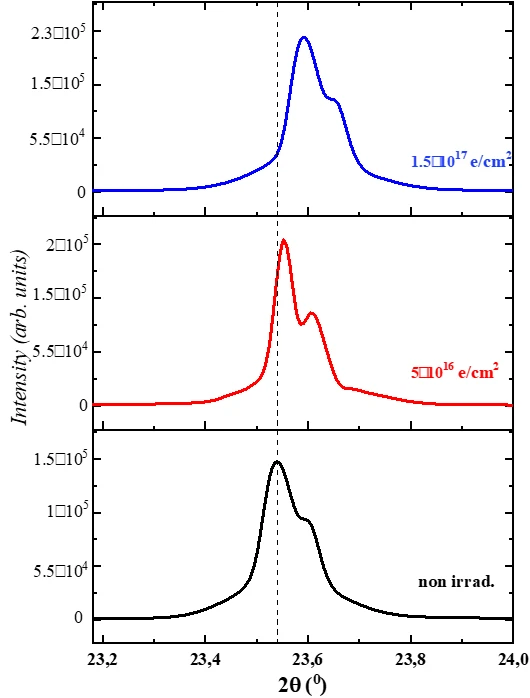
Figure 3. Shift of the peak (004) towards larger angles depending on the radiation flux density
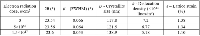
Table 1. The results of the structural characteristics of the TlGaS2 single crystal irradiated with accelerated electrons
TlGaS₂ crystallizes in the monoclinic space group C2/c. There are two nonequivalent nodes Tl¹⁺. At the first Tl¹⁺ site, Tl¹⁺ is bonded in 8-coordinate geometry to eight S²⁻ atoms, with Tl–S bond distances ranging from 3.28 to 3.75 Å. At the second Tl¹⁺ site, Tl¹⁺ is also bonded in 8-coordinate geometry to eight S²⁻ atoms, with Tl–S bond distances ranging from 3.27 to 3.73 Å. There are two nonequivalent Ga³⁺ sites. At the first Ga³⁺ site, Ga³⁺ is bonded to four S²⁻ atoms, forming corner-sharing GaS₄ tetrahedra. The Ga–S bond lengths are three shorter bonds at 2.28 Å and one longer bond at 2.29 Å. At the second Ga³⁺ site, Ga³⁺ is also bonded to four S²⁻ atoms, forming corner-sharing GaS₄ tetrahedra. The Ga–S bond lengths include two shorter bonds at 2.28 Å and two longer bonds at 2.29 Å. There are five nonequivalent S²⁻ sites:
At the first S²⁻ site, S²⁻ is bound in a distorted water-like geometry to four Tl¹⁺ atoms and two Ga³⁺ atoms. At the second S²⁻ site, S²⁻ is also bound in a distorted water-like geometry to four Tl¹⁺ atoms and two Ga³⁺ atoms. In the third S²⁻ site, S²⁻ is similarly bound in a distorted water-like geometry with four Tl¹⁺ atoms and two Ga³⁺ atoms. In the fourth S²⁻ site, S²⁻ is bonded in a distorted water-like geometry to four Tl¹⁺ atoms and two equivalent Ga³⁺ atoms. In the fifth S²⁻ site, S²⁻ is also bonded in a distorted water-like geometry to four Tl¹⁺ atoms and two equivalent Ga³⁺ atoms. It was found that after irradiation of a TlGaS2 single crystal with electrons at a fluence of 1.5×10¹⁷ elektron/cm2, the initial structure is preserved. In this case, the unit cell parameters before irradiation are a = 10 Å, b= 10 Å, c= 14.973 Å. After irradiation, a= 10 Å, b= 10 Å, c= 14.968 Å.
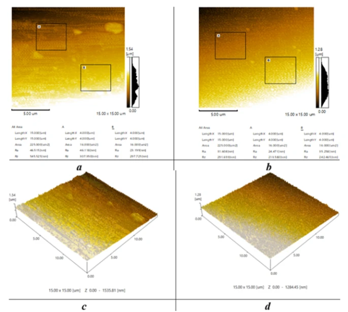
Figure 5. AFM images of the initial TlGaS2 (a, c) and (b, d) irradiated with electrons with a fluence of 1.5×10¹⁷ electrons/cm2
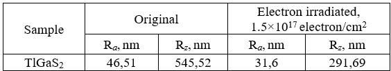
Table 2. The results of the AFM study of the surface microrelief of the TlGaS2 single crystal before and after irradiation with accelerated electrons
Changes in the microrelief of the surface of a TlGaS2 single crystal under electron irradiation with a flux of 1.5×10¹⁷ electrons/cm2 were studied using an atomic force microscope (AFM).
The results of the AFM study of the surface microrelief of the TlGaS2 single crystal before and after irradiation with accelerated electrons are presented in figure 5, and also in table 2. The study was conducted without any pre-treatment. According to the data obtained, electron irradiation of TlGaS2 significantly changes the surface morphology: leads to a decrease in the maximum value of the arithmetic mean deviation of the profile from Ra = 46.51 nm, before irradiation Ra = 31.6 nm, as well as to a decrease in the average roughness from Rz = 545.52 nm before irradiation Rz = 291.69 nm.
Electron irradiation has a significant effect on the structure and surface morphology of TlGaS2 single crystals. Thus, the experimental results show that electron irradiation significantly improved the surface condition of TlGaS2 crystals. It was found that after irradiation of a TlGaS2 single crystal with electrons at a fluence of 1.5×10¹⁷ electron/cm2, the original structure is preserved. yUnderstanding the relationship between electron radiation and the properties of TlGaS2 is critical to advancing its use in high-performance devices. As the demand for materials that can withstand radiation exposure increases, continued research in this area will help pave the way for the development of more resilient and reliable materials for a variety of technological applications.
1 R.M. Sardarly, F.T. Salmanov, N.A. Aliyeva, R.N. Mehdiyeva, S.M. Gakhramanova, Modern Physics Letters B 35 (2021) 2150504. https://doi.org/10.1142/S0217984921505047
2 M.Yu. Tashmetov, F.K. Khallokov, N.B. Ismatov, I.I. Yuldashova, I. Nuritdinov, S.Kh. Umarov, Physica B: Condensed Matter 613 (2021) 412879. https://doi.org/10.1016/j.physb.2021.412879
3 R.M. Sardarly, G.M. Ashirov, L.F. Mashadiyeva, N.A. Aliyeva, F.T. Salmanov, R.Sh. Agayeva, R.A. Mamedov, M.B. Babanly, Modern Physics Letters B 36(32-33) (2022) 2250171. https://doi.org/10.1142/S0217984922501718
4 S.Kh. Umarov, N.Z. Gasanov, F.K. Khallokov, Eurasian Union of Scientists 4(49) (2018) 27.
5 M. Isik, E. Bulur, N.M. Gasanly, Journal of Luminescence 135 (2013) 60. https://doi.org/10.1016/j.jlumin.2012.10.025
6 T.G. Naghiyev, R.F. Babayeva, A.S. Abdinov, Current Applied Physics 80 (2025) 176. https://doi.org/10.1016/j.cap.2025.09.019
7 A.S. Abdinov, R.F. Babayeva, T.G. Naghiyev, International Journal of Modern Physics B 39(21) (2025) 2550194. https://doi.org/10.1142/S0217979225501942
8 A.Sh. Abdinov, R.F. Babayeva, S.I. Amirova, N.A. Rahimova, E.A. Rasulov, UNEC Journal of Engineering and Applied Sciences 5(1) (2025) 55. https://doi.org/10.61640/ujeas.2025.0506
9 A.S. Abdinov, R.F. Babayeva, Y.I. Aliyev, International Journal of Modern Physics B, 39(12) (2025) 2550089. https://doi.org/10.1142/S0217979225500894
10 G.S. Hadjieva, K.O. Taghiyev, E.G. Asadov, F.A. Kazimova, T.Sh Ibragimova, O. B. Tagiyev, Mod. Phys. Lett. B 34(31) (2020) 2050344. https://doi.org/10.1142/%20S0217984920503443
11 E.G. Asadov, O.B. Tagiev, G.S. Gadzhieva, A.H. Asadova, B.D. Urmanov, M.S. Leonenya, G.P. Yablonskii, Solid State Commun. 356 114933 (2022). https://doi.org/10.1016/j.ssc.2022.114933
12 B.D. Urmanov, M.S. Leanenia, G.P. Yablonskii, O.B. Tagiev, E.G. Asadov, Journal of Applied Spectroscopy 90 (2023) 595. https://doi.org/10.1007/s10812-023-01570-2
13 T.G. Naghiyev, R.M. Rzayev, Modern Physics Letters B 35(31) (2021) 2150469. https://doi.org/10.1142/S0217984921504698
14 T.G. Naghiyev, Modern Physics Letters B (37)12 (2023) 2350021. https://doi.org/10.1142/S0217984923500215
15 T.D. Ibragimov, A.M. Hashimov, G.B. Ibragimov, R.M. Rzayev, Fullerenes, Nanotubes and Carbon Nanostructures 29(12) (2021) 951. https://doi.org/10.1080/1536383X.2021.1920579
16 M.S. Leanenya, E.V. Lutsenko, V.N. Pavlovskii, G.P. Yablonskii, T.G. Nagiev, B.G. Tagiev, O.B. Tagiev, S.A. Abushev, J. Appl. Spectrosc. 82 (2015) 53 . https://doi.org/10.1007/s10812-015-0063-6
17 17. F. Behmagham, S. Arshadi, E. Vessally, T.G. Naghiyev, R. Rzayev, D. Sur, S. Ganesan, Computational and Theoretical Chemistry 1243 (2025) 114976. https://doi.org/10.1016/j.comptc.2024.114976
18 M.S. Leanenia, E.V. Lutsenko, M.V. Rzheutski, G.P. Yablonskii, T.G. Naghiyev, O.B. Tagiev, J. Appl. Phys. 129 (2021) 243104. https://doi.org/10.1063/5.0051319
19 S.G. Asadullayeva, N.A. Ismayilova, T.G. Naghiyev, Modern Physics Letters B 37(34) (2023) 2350166. https://doi.org/10.1142/S021798492350166X
20 R.S. Madatov, A.S. Alekperov, N.N. Gadzhieva, F.G. Asadov, Sh.A. Allahverdiev, E.G. Asadov, T.G. Naghiyev, International Journal of Modern Physics B 33(09) (2019) 1950066. https://doi.org/10.1142/S0217979219500668
21 M. Isik, E. Bulur, N.M. Gasanly, Journal of Luminescence 244 (2022) 118714. https://doi.org/10.1016/j.jlumin.2021.118714
22 P.H. Ismayilova, N.Z. Gasanov, A.A. Hajiyeva, Semiconductors 59(2) (2025) 162. https://doi.org/10.1134/S1063782625600500
23 M.Yu. Tashmetov, F.K. Khallokov, N.B. Ismatov, I.I. Yuldashova, S.Kh. Umarov, International Journal of Modern Physics B 35(28) (2021) 2150289. https://doi.org/10.1142/S0217979221502891
24 M.Yu. Tashmetov, F.K. Khallokov, N.B. Ismatov, S.Kh. Umarov, Uzbek Journal of Physics 23(4) (2021) 51.
25 S.M. Asadov, S.N. Mustafaeva, Inorganic Materials 60 (2024) 1283. https://doi.org/10.1134/S0020168525700098
26 S.H. Umarov, N.Z. Hasanov, F.K. Khallokov, Z.M. Narzullaeva, Scientific Reports of Bukhara State University 35(3) (2023) 16.
27 I. Nuritdinov, M.Yu. Tashmetov, U.O. Khodzhaev, S.Kh. Umarov, F.K. Khallokov, Eurasian Physical Technical Journal 20(4) (2023) 23. https://doi.org/10.31489/2023No4/23-32
28 K.M. Guseinova, F.A. Mammadov, A.A. Hadiyeva, V.I. Eminova, C.I. Huseynov, East European Journal of Physics (4) (2024) 322. https://doi.org/10.26565/2312-4334-2024-4-36
29 M. Isik, A. Karatay, A.N. Ech-Chergui, N.M. Gasanly, Physica Scripta 97 (2022) 075808. https://iopscience.iop.org/article/10.1088/1402-4896/ac74f0
30 F.K. Khallokov, G.T. Imanova, S.Kh. Umarov, M.Yu. Tashmetov, N.Z. Gasanov, Z.U. Esanov, I.R. Bekpulatov, Materials Research Innovations 28(4) (2024) 1. https://doi.org/10.1080/14328917.2024.2363583
31 S.Kh. Umarov, F.K. Khallokov, Eurasian Union of Scientists 6(51) (2018) 38.
32 T.D. Ibrahimov, I.I. Aslanov, Solid State Communications 123(8) (2002) 339. https://doi.org/10.1016/S0038-1098(02)00324-1
33 N.M. Gasanly, Journal of the Korean Physical Society 57(1) (2010) 164. https://doi.org/10.3938/jkps.57.164
34 M. Hanias, A.N. Anagnostopoulos, K. Kambas, J. Spyridelis, Materials Research Bulletin 27(1) (1992) 25. https://doi.org/10.1016/0025-5408(92)90039-3
35 F.K. Khallokov, M.T. Normuradov, Sh.T. Khozhiev, K.T. Dovranov, Kh.T. Davranov, M.A. Davlatov, Ukrainian Journal of Physics 68(3) (2023) 210. https://doi.org/10.15407/ujpe68.3.210
36 B.B. Gaibnazarov, G. Imanova, Sh.T. Khozhiev, I.O. Kosimov, I.Kh. Khudaikulov, Sh.K. Kuchkanov, F.K. Khallokov, I.R. Bekpulatov, Integrated Ferroelectrics 237(1) (2023) 208. https://doi.org/10.1080/10584587.2023.2239097
37 M.N. Mirzayev, G.T. Imanova, D. Neov, M. Rasul, I.R. Bekpulatov, F.K. Khallokov, E.P. Popov, K. Hasanov, S. Ismayilova, B. Mauyey, D.M. Mirzayeva, F. Tatardar, M. Dinu, G. Kaminski, A. Vladescu (Dragomir), Journal of Porous Materials 31(4) (2024) 1531. https://doi.org/10.1007/s10934-024-01627-3
38 S.K. Umarov, I. Nuritdinov, Z.Z. Ashurov, F.K. Khallokov, Technical Physics 64 (2019) 183. https://doi.org/10.1134/S1063784219020257
39 S.K. Umarov, I. Nuritdinov, Z.D. Ashurov, F.K. Khallokov, Technical Physics Letters 43 (2017) 730. https://doi.org/10.1134/S1063785017080260
40 I. Khidirov, I.J. Jaksimuratov, F.K. Khallokov, Industrial Laboratory, Diagnostics of Materials 90(3) (2024) 32. https://doi.org/10.26896/1028-6861-2024-90-3-32-38
41 M.Yu. Tashmetov, B.N. Madaminov, N.B. Ismatov, F.K. Khallokov, B.A. Abdikamalov, International Journal of Modern Physics B 39(13) (2025) 2550103. https://dx.doi.org/10.1142/S0217979225501036
42 R.M. Sardarli, F.T. Salmanov, N.A. Alieva, R.M. Abbasli, Modern Physics Letters B 34(11) (2020) 2050113. https://doi.org/10.1142/S0217984920501134
S.Kh. Umarov, G.T. Imanova, N.Z. Gasanov, F.K. Khallokov, Z.M. Narzullaeva, S.S. Davlatov, R.R. Hamroyev, Kh.Z. Salomova, O.B. Rakhmatov, A.Sh. Rashidov, I.R. Bekpulatov, A.M. Ahmadova, Influence of electron irradiation on structural and surface - morphological properties of TlGaS2 monocrystal, UNEC J. Eng. Appl. Sci. 5(2) (2025) 88-97. https://doi.org/10.61640/ujeas.2025.1207
Anyone you share the following link with will be able to read this content:
This article is licensed under the Creative Commons Attribution ( CC BY 4.0 ) License, which permits unrestricted use, distribution, and reproduction in any medium, provided the original author and source are credited.
R.M. Sardarly, F.T. Salmanov, N.A. Aliyeva, R.N. Mehdiyeva, S.M. Gakhramanova, Modern Physics Letters B 35 (2021) 2150504. https://doi.org/10.1142/S0217984921505047
M.Yu. Tashmetov, F.K. Khallokov, N.B. Ismatov, I.I. Yuldashova, I. Nuritdinov, S.Kh. Umarov, Physica B: Condensed Matter 613 (2021) 412879. https://doi.org/10.1016/j.physb.2021.412879
R.M. Sardarly, G.M. Ashirov, L.F. Mashadiyeva, N.A. Aliyeva, F.T. Salmanov, R.Sh. Agayeva, R.A. Mamedov, M.B. Babanly, Modern Physics Letters B 36(32-33) (2022) 2250171. https://doi.org/10.1142/S0217984922501718
S.Kh. Umarov, N.Z. Gasanov, F.K. Khallokov, Eurasian Union of Scientists 4(49) (2018) 27.
M. Isik, E. Bulur, N.M. Gasanly, Journal of Luminescence 135 (2013) 60. https://doi.org/10.1016/j.jlumin.2012.10.025
T.G. Naghiyev, R.F. Babayeva, A.S. Abdinov, Current Applied Physics 80 (2025) 176. https://doi.org/10.1016/j.cap.2025.09.019
A.S. Abdinov, R.F. Babayeva, T.G. Naghiyev, International Journal of Modern Physics B 39(21) (2025) 2550194. https://doi.org/10.1142/S0217979225501942
A.Sh. Abdinov, R.F. Babayeva, S.I. Amirova, N.A. Rahimova, E.A. Rasulov, UNEC Journal of Engineering and Applied Sciences 5(1) (2025) 55. https://doi.org/10.61640/ujeas.2025.0506
A.S. Abdinov, R.F. Babayeva, Y.I. Aliyev, International Journal of Modern Physics B, 39(12) (2025) 2550089. https://doi.org/10.1142/S0217979225500894
G.S. Hadjieva, K.O. Taghiyev, E.G. Asadov, F.A. Kazimova, T.Sh Ibragimova, O. B. Tagiyev, Mod. Phys. Lett. B 34(31) (2020) 2050344. https://doi.org/10.1142/%20S0217984920503443
E.G. Asadov, O.B. Tagiev, G.S. Gadzhieva, A.H. Asadova, B.D. Urmanov, M.S. Leonenya, G.P. Yablonskii, Solid State Commun. 356 114933 (2022). https://doi.org/10.1016/j.ssc.2022.114933
B.D. Urmanov, M.S. Leanenia, G.P. Yablonskii, O.B. Tagiev, E.G. Asadov, Journal of Applied Spectroscopy 90 (2023) 595. https://doi.org/10.1007/s10812-023-01570-2
T.G. Naghiyev, R.M. Rzayev, Modern Physics Letters B 35(31) (2021) 2150469. https://doi.org/10.1142/S0217984921504698
T.G. Naghiyev, Modern Physics Letters B (37)12 (2023) 2350021. https://doi.org/10.1142/S0217984923500215
T.D. Ibragimov, A.M. Hashimov, G.B. Ibragimov, R.M. Rzayev, Fullerenes, Nanotubes and Carbon Nanostructures 29(12) (2021) 951. https://doi.org/10.1080/1536383X.2021.1920579
M.S. Leanenya, E.V. Lutsenko, V.N. Pavlovskii, G.P. Yablonskii, T.G. Nagiev, B.G. Tagiev, O.B. Tagiev, S.A. Abushev, J. Appl. Spectrosc. 82 (2015) 53 . https://doi.org/10.1007/s10812-015-0063-6
17. F. Behmagham, S. Arshadi, E. Vessally, T.G. Naghiyev, R. Rzayev, D. Sur, S. Ganesan, Computational and Theoretical Chemistry 1243 (2025) 114976. https://doi.org/10.1016/j.comptc.2024.114976
M.S. Leanenia, E.V. Lutsenko, M.V. Rzheutski, G.P. Yablonskii, T.G. Naghiyev, O.B. Tagiev, J. Appl. Phys. 129 (2021) 243104. https://doi.org/10.1063/5.0051319
S.G. Asadullayeva, N.A. Ismayilova, T.G. Naghiyev, Modern Physics Letters B 37(34) (2023) 2350166. https://doi.org/10.1142/S021798492350166X
R.S. Madatov, A.S. Alekperov, N.N. Gadzhieva, F.G. Asadov, Sh.A. Allahverdiev, E.G. Asadov, T.G. Naghiyev, International Journal of Modern Physics B 33(09) (2019) 1950066. https://doi.org/10.1142/S0217979219500668
M. Isik, E. Bulur, N.M. Gasanly, Journal of Luminescence 244 (2022) 118714. https://doi.org/10.1016/j.jlumin.2021.118714
P.H. Ismayilova, N.Z. Gasanov, A.A. Hajiyeva, Semiconductors 59(2) (2025) 162. https://doi.org/10.1134/S1063782625600500
M.Yu. Tashmetov, F.K. Khallokov, N.B. Ismatov, I.I. Yuldashova, S.Kh. Umarov, International Journal of Modern Physics B 35(28) (2021) 2150289. https://doi.org/10.1142/S0217979221502891
M.Yu. Tashmetov, F.K. Khallokov, N.B. Ismatov, S.Kh. Umarov, Uzbek Journal of Physics 23(4) (2021) 51.
S.M. Asadov, S.N. Mustafaeva, Inorganic Materials 60 (2024) 1283. https://doi.org/10.1134/S0020168525700098
S.H. Umarov, N.Z. Hasanov, F.K. Khallokov, Z.M. Narzullaeva, Scientific Reports of Bukhara State University 35(3) (2023) 16.
I. Nuritdinov, M.Yu. Tashmetov, U.O. Khodzhaev, S.Kh. Umarov, F.K. Khallokov, Eurasian Physical Technical Journal 20(4) (2023) 23. https://doi.org/10.31489/2023No4/23-32
K.M. Guseinova, F.A. Mammadov, A.A. Hadiyeva, V.I. Eminova, C.I. Huseynov, East European Journal of Physics (4) (2024) 322. https://doi.org/10.26565/2312-4334-2024-4-36
M. Isik, A. Karatay, A.N. Ech-Chergui, N.M. Gasanly, Physica Scripta 97 (2022) 075808. https://iopscience.iop.org/article/10.1088/1402-4896/ac74f0
F.K. Khallokov, G.T. Imanova, S.Kh. Umarov, M.Yu. Tashmetov, N.Z. Gasanov, Z.U. Esanov, I.R. Bekpulatov, Materials Research Innovations 28(4) (2024) 1. https://doi.org/10.1080/14328917.2024.2363583
S.Kh. Umarov, F.K. Khallokov, Eurasian Union of Scientists 6(51) (2018) 38.
T.D. Ibrahimov, I.I. Aslanov, Solid State Communications 123(8) (2002) 339. https://doi.org/10.1016/S0038-1098(02)00324-1
N.M. Gasanly, Journal of the Korean Physical Society 57(1) (2010) 164. https://doi.org/10.3938/jkps.57.164
M. Hanias, A.N. Anagnostopoulos, K. Kambas, J. Spyridelis, Materials Research Bulletin 27(1) (1992) 25. https://doi.org/10.1016/0025-5408(92)90039-3
F.K. Khallokov, M.T. Normuradov, Sh.T. Khozhiev, K.T. Dovranov, Kh.T. Davranov, M.A. Davlatov, Ukrainian Journal of Physics 68(3) (2023) 210. https://doi.org/10.15407/ujpe68.3.210
B.B. Gaibnazarov, G. Imanova, Sh.T. Khozhiev, I.O. Kosimov, I.Kh. Khudaikulov, Sh.K. Kuchkanov, F.K. Khallokov, I.R. Bekpulatov, Integrated Ferroelectrics 237(1) (2023) 208. https://doi.org/10.1080/10584587.2023.2239097
M.N. Mirzayev, G.T. Imanova, D. Neov, M. Rasul, I.R. Bekpulatov, F.K. Khallokov, E.P. Popov, K. Hasanov, S. Ismayilova, B. Mauyey, D.M. Mirzayeva, F. Tatardar, M. Dinu, G. Kaminski, A. Vladescu (Dragomir), Journal of Porous Materials 31(4) (2024) 1531. https://doi.org/10.1007/s10934-024-01627-3
S.K. Umarov, I. Nuritdinov, Z.Z. Ashurov, F.K. Khallokov, Technical Physics 64 (2019) 183. https://doi.org/10.1134/S1063784219020257
S.K. Umarov, I. Nuritdinov, Z.D. Ashurov, F.K. Khallokov, Technical Physics Letters 43 (2017) 730. https://doi.org/10.1134/S1063785017080260
I. Khidirov, I.J. Jaksimuratov, F.K. Khallokov, Industrial Laboratory, Diagnostics of Materials 90(3) (2024) 32. https://doi.org/10.26896/1028-6861-2024-90-3-32-38
M.Yu. Tashmetov, B.N. Madaminov, N.B. Ismatov, F.K. Khallokov, B.A. Abdikamalov, International Journal of Modern Physics B 39(13) (2025) 2550103. https://dx.doi.org/10.1142/S0217979225501036
R.M. Sardarli, F.T. Salmanov, N.A. Alieva, R.M. Abbasli, Modern Physics Letters B 34(11) (2020) 2050113. https://doi.org/10.1142/S0217984920501134