UNEC Journal of Engineering and Applied Sciences Volume 5, No 2, pages 98-103 (2025) Cite this article, ![]() 564 https://doi.org/10.61640/ujeas.2025.1208
564 https://doi.org/10.61640/ujeas.2025.1208
The rapid advancement of techniques and electronics necessitated enhancements in manufacturing processes, design methodologies, and material usage [1-7]. Semimagnetic semiconductors (SMSC) have considerable interest in recent decades due to their unique combination of semiconducting and magnetic properties. These materials offer promising opportunities for the development of novel electronic and spintronic devices, in which both the charge and spin of electrons are utilized for information processing and storage [8-11].
Among the SMSC, IV–VI group compounds such as PbTe doped with transition metal ions, including Fe, have emerged as important model systems for studying spin-dependent phenomena in narrow-gap semiconductors. PbTe is a well-known narrow-gap semiconductor with excellent thermoelectric and optical properties, widely used in infrared detectors and thermoelectric devices [12].
Alloys based on PbTe that contain transition 3d metal impurities with variable valence states (such as Sc, Mn, Ti, Cr, and Fe) exhibit deep energy levels near the band gap. These alloys are SMSC whose magnetic behavior depends not only on the concentration of impurities but also on their electronic structure [8-19].
When doped with Fe² ions, the resulting compound Pb1-xFeₓTe exhibits semimagnetic behavior due to the interaction between the localized magnetic moments of Fe ions and the delocalized carriers in the host lattice. These interactions lead to modifications in the electronic band structure and introduce new energy levels associated with the 3d orbitals of Fe2+ ions, affecting both the transport and optical properties of the material [20-24].
Although iron-doped PbTe single crystals were first synthesized over 30 years ago, there are still only a limited number of studies focused on the physical properties of Pb1-xFeₓTe alloys [19,23-25]. Most of the existing research has concentrated primarily on their magnetic characteristics [19,24], while details regarding their electrical behavior and electronic structure remain scarce. It has been shown that these materials typically exhibit p-type conductivity and display paramagnetic behavior, with iron having a relatively low solubility in the host lattice (up to approximately 0.15 mol%).
Pb1-xFeₓTe solid solutions represent a promising class of semiconductor materials with unique magnetic and optical properties. The incorporation of iron (Fe) ions into the PbTe lattice enables the formation of semimagnetic semiconductors, which are used in spintronics, magnetic sensors, and other high-tech applications. The epitaxial growth of such materials on various substrates is a key step in obtaining high-quality films with tailored properties.
PbTe is a narrow-bandgap (Eg≈0.31eV) semiconductor with a cubic NaCl-type lattice. Partial substitution of Pb with Fe ions leads to changes in the electronic structure and the emergence of magnetic interactions associated with the local moments of Fe. However, due to differences in the size and chemical activity of Fe ions, certain difficulties arise in forming uniform solid solutions.
PbTe have a cubic face-centered crystal lattice with a lattice constant aPbTe=6.46 Å and for FeTe aFeTe ≈5.27 Å . The creation of various devices and multi-element matrices requires the production of films with high crystalline perfection and reproducible electrophysical parameters.
As Fe2+ ions substitute Pb²⁺(≈1.19 Å) ions, the ionic radius of Fe (≈0.78 Å) is smaller compared to that of Pb²⁺, which leads to the formation of strain in the crystal lattice and, as a result, the lattice constant tends to decrease. According to Vegard's law [26-30]:

The paper aims to study the optimal regime for obtaining perfect samples of Pb1-xFeₓTe epitaxial films and study their optical properties. In this study, the growth, structural characteristics, and optical properties of Pb1-xFeₓTe (x < 0.05) epitaxial films grown on BaF2 substrates using the molecular beam condensation method were investigated. Special attention is given to the optimization of growth conditions to achieve high structural quality and to understand how increasing Fe content influences the material’s band structure and optical behavior. The results provide insights into the fundamental properties of Pb1-xFeₓTe and contribute to the broader understanding of SMSC for potential applications in optoelectronics and spintronics.
In this paper, we consider the study of the growth and structure properties of epitaxial films Pb1-xFexTe (x=0.05) with a thickness of 0.5¸1 µm, grown on BaF2 substrates, by the molecular beam condensation method in a vacuum of 10-4 Pa on a standard vacuum unit УBН-71П-3 with the use of an additional compensating source of Te vapor during growth process. Synthesized solid solutions Pb1-xFexTe (x=0.05) were used as a source. The evaporator of the starting materials was a Knudsen cell made of extra pure graphite.
The optimal conditions for obtaining structurally perfect Pb1-xFeₓTe epitaxial films were determined as follows: substrate temperature Tsubst=573÷623 K, Tsourc = 1123÷1173 K. For obtaining of perfect samples, it was used compensating source of Te and the temperature of it was TTe=410 K. The condensation speed was Jc =8¸9 Å/sеc.
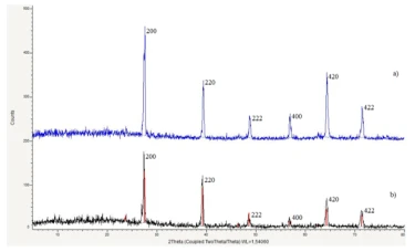
The crystal structure was assessed using an X-ray diffractometer (XRD) in the using a Bruker XRD D8 Advance diffractometer with filtered CuKα radiation. It has been established that, under these conditions, perfect films are obtained along the <200>, <220>, <222>, <400>, <420>, <422> growth direction. In figure 1a, b was performed XRD analysis of PbTe and Pb1-xFeₓTe (x=0.05) solid solution respecivly. The lattice parameter of Pb1-xFeₓTe (x = 0.05) epitaxial layers was calculated and found to be a=6.37 A˚ according to XRD analysis. Thus, the lattice parameter of Pb1-xFeₓTe decrese with increasing of Fe2+ ions concentration.
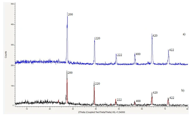
Figure 1. X-ray diffraction patterns epitaxial films at Тsub=573¸623 K a) PbTe, b) Pb1-xFexTe (x=0.05)
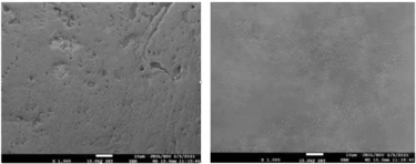
The surface morphology of the films was analyzed with a scanning electron microscope (SEM) method using JEOL JSM-7600F Field Emission SEM. SEM images revealed the presence of black clusters characteristic of lead chalcogenides [24,25,28] (figure 2a). The black patterns disappear with using of additional compensating Te sources at TTe=410 K (figure 2b).
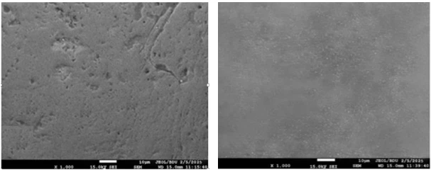
Figure 2. SEM images of the surface of Pb1–xFexTe epitaxial films (х=0.05) grown on BaF2 substrates, Тsub=573¸623 K; TTe=410 K, a) without Te compensation, b) after Te compensation
a) b)
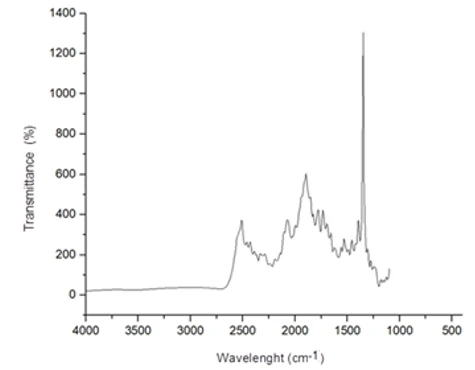
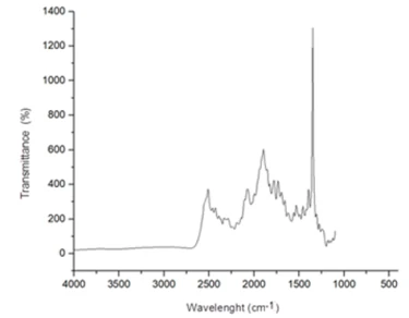
As a continuation of the research, the optical properties of the obtained films were studied by Fourier Transform Infrared (FT-IR) spectroscopy method using an IR Affinity-1 FT-IR spectrometer (Shimadzu, Japan). Transmittance spectra were recorded in the wavenumber range of 350–4000 cm-1 at room temperature (figure 3). The investigations and calculations revealed that a sharp increase begins approximately at the wavenumber around 2260 cm-1. This corresponds to the onset of the band gap. For the wavenumber (ν ≈ 2260 cm-1):
 (2)
(2)
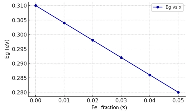
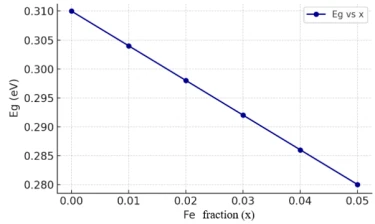
The band gap value of Pb1–xFexTe for х=0.03was Eg=0.29 eV and for х=0.05 was Eg=0.28 eV, typically corresponds to the infrared range, making it suitable for IR detectors or thermoelectric applications. As seen from figure 4 and table 1, increasing the Fe content leads to a reduction of the band gap compared to PbTe (Eg≈0.31eV).
The main reasons for the decrease in the bandgap in Pb1–xFexTe as the Fe content (x) increases are as follows: Fe2+ ions, when incorporated into the PbTe crystal lattice, create localized levels associated with the 3d orbitals of Fe2+ ions, which are located close to the valence and conduction bands. These localized levels interact with the band structure, resulting in a reduction of the bandgap.
Furthermore, the magnetic Fe2+ ions induce magnetic interactions that can lead to band splitting and a decrease in the Eg.
Thus, by adding Fe ions to PbTe semicondictor, due to the emergence of localized levels and the strengthening of sp-d interactions, the band gap decreases.
The study successfully established the optimal growth conditions for high-quality Pb1–xFexTe (x < 0.05) epitaxial films with thicknesses ranging from 0.5 to 1 µm, grown on BaF2 substrates using molecular beam epitaxy in a high vacuum. The optimal parameters were identified as substrate temperature Тsub = 573¸623 K, tellurium source temperature TTe=410 K, and growth rate Jc =8¸9 Å/sеc.
Structural characterization via XRD confirmed the formation of epitaxial films with high crystalline perfection, with the lattice parameter determined to be approximately a = 6.37 A˚. SEM analysis revealed surface morphology features sensitive to growth parameters, including the presence of lead chalcogenide clusters, which increased at lower condensation rates and higher substrate temperatures.
Optical studies revealed that an increase in Fe concentration results in a decrease in the band gap, attributed to the emergence of localized 3d orbitals of Fe²⁺ ions and enhanced sp–d exchange interactions. The band gap value positions these films within the infrared spectral range, indicating their potential suitability for infrared detector and thermoelectric applications.
Overall, this research offers valuable insights into the synthesis, structural characteristics, and optoelectronic properties of Pb₁₋ₓFeₓTe epitaxial films, supporting their promising application in advanced spintronic and infrared optoelectronic devices.
1 N.R. Rahmanov, V.G. Kurbatsky, H.B. Guliyev, N.V. Tomin, A.F. Yaqubov, Rudenko International Conference on Methodological Problems in Reliability Study of Large Energy Systems 461 (2023) 01023.
2 A.M. Hashimov, N.M. Rahmanov, N.M. Tabatabaei, H.B. Guliyev, F.Sh. Ibrahimov, International Journal on Technical and Physical Problems of Engineering 12(2) (2020) 40.
3 A.O. Mekhrabov, E.A. Irmak, M.V. Akdeniz, R.M. Rzaev, UNEC J. Eng. Appl. Sci. 5(1) (2025) 43. https://doi.org/10.61640/ujeas.2025.0505
4 A.I. Isayev, S.I. Mekhtiyeva, H.I. Mammadova, R.I. Alekberov, Q.M. Ahmadov, N.N. Eminova, A.Ch. Mammadova, L.A. Aliyeva, L.V. Afandiyeva, R.F. Sadikhli, UNEC J. Eng. Appl. Sci. 4(1) (2024) 55. https://doi.org/10.61640/ujeas.2024.0505
5 T.G. Naghiyev, E.M. Huseynov, UNEC J. Eng. Appl. Sci. 3(1) 2023 10. https://doi.org/10.61640/ujeas.2023.0502
6 B.G. Ibrahimov, A.A. Alieva, Advances in Intelligent Systems and Computing 1306 (2021) 773.
7 B. Ibrahimov, Transport and Telecommunication 24(4) (2023) 375.
8 J.K. Furdyna, Journal of Applied Physics 64(4) (1988) R29.
9 R.F. Babayeva, A.Sh. Abdinov, S.I. Amirova, N.A. Ragimova, E.A. Rasulov, UNEC J. Eng. Appl. Sci. 3(1) (2023) 5. https://doi.org/10.61640/ujeas.2023.0501
10 A.S. Huseynova, F.F. Yahyayev, UNEC J. Eng. Appl. Sci. 2(2) (2022) 29.
11 I. Žutić, J. Fabian, S. Das Sarma, Reviews of Modern Physics 76(2) (2004) 323.
12 Y.I. Ravich, B.A. Efimova, I.A. Smirnov, Semiconducting Lead Chalcogenides, Springer US (1970).
13 M.A. Mehrabova, R.M. Sadigov, I.R. Nuriyev, A.M. Nazarov, International Journal of Modern Physics B 38(3) (2024) 2450419.
14 M.A. Mehrabova, N.H. Hasanov, V.G. Guluzade, R.M. Sadigov, WSEAS Transactions on Electronics 13 (2022) 23.
15 R.F. Babayeva, A.Sh. Abdinov, N.A. Ragimova, S.I. Amirova, E.A. Rasulov, UNEC J. Eng, Appl. Sci. 1(1) (2021) 22.
16 R.I. Alekberov, A.I. Isayev, S.I. Mekhtiyeva, Margit Fabián, UNEC J. Eng. Appl. Sci. 1(1) (2021) 27.
17 A.Sh. Abdinov, R.F. Babayeva, S.I. Amirova, N.A. Rahimova, E.A. Rasulov, UNEC J. Eng. Appl. Sci. 5(1) (2025) 55. https://doi.org/10.61640/ujeas.2025.0506
18 M.A. Mehrabova, H.R. Nuriyev, T.I. Kerimova, N.H. Hasanov, R.M. Sadigov, A.A. Abdullayeva, Engineering World (2020) 247.
19 E.P. Skipetrova, A.A. Soloveva, V.E. Slynko, Semiconductors 52(6) (2018) 686.
20 Y.H. Zeng, J.B. Xia, Physical Review B 72(19) (2005) 195204. https://doi.org/10.1103/PhysRevB.72.195204
21 E.P. Skipetrova, A.V. Knotko, E.I. Slynko, V.E. Slynko, Low Temperature Physics 41 (2015) 141.
22 D.T. Morelli, J.P. Heremans, C.M. Thrush, Physical Review B 67 (2003) 035206.
23 M.A. Mehrabova, H.R. Nuriyev, H.S. Orujov, N.H. Hasanov, T.I. Kerimova, A.A. Abdullayeva, A.I. Kazimova, Physics of the Solid State 61 (2019) 2306.
24 A.O. Mekhrabov, M.A. Mehrabova, Materials Science Forum 1119 (2024) 3.
25 M.A. Mehrabova, N.T. Panahov, N.H. Hasanov, Materials Physics and Mechanics 48(3) (2022) 419.
26 M. Ameria, D. Racheda, M. Rabaha, R. Khenataa, N. Benkhettoua, B. Bouhafsd, M. Maachouc, Materials Science in Semiconductor Processing 10 (2007) 6.
27 Ch.I. Abilov, P.G. Rustamov, S.G. Agdamskaya, Journal of Inorganic Chemistry 31(6) (1986) 1516.
28 T. Story, Optoelectronic Properties of Semiconductors and Superlattices, Taylor & Francis, New York–London 18 (2003) 385.
29 M.A. Jafarov, V.M. Salmanov, A.H. Huseynov, R.M. Mamedov, T.A. Mamedova, F.S. Ahmedova, A.B. Aliyeva, UNEC J. Eng. Appl. Sci. 3(2) (2023) 54. https://doi.org/10.61640/ujeas.2023.1207
30 T.G. Naghiyev, U.R. Rzayev, E.M. Huseynov, I.T. Huseynov, S.H. Jabarov, UNEC J. Eng. Appl. Sci 2(1) (2022) 85.
M.A. Mehrabova, R.М. Sadigov, K.E. Rahimova, Growth, structural and optical properties of Pb1-xfeₓTe epitaxial films, UNEC J. Eng. Appl. Sci. 5(2) (2025) 98-103. https://doi.org/10.61640/ujeas.2025.1208
Anyone you share the following link with will be able to read this content:
This article is licensed under the Creative Commons Attribution ( CC BY 4.0 ) License, which permits unrestricted use, distribution, and reproduction in any medium, provided the original author and source are credited.


N.R. Rahmanov, V.G. Kurbatsky, H.B. Guliyev, N.V. Tomin, A.F. Yaqubov, Rudenko International Conference on Methodological Problems in Reliability Study of Large Energy Systems 461 (2023) 01023.
A.M. Hashimov, N.M. Rahmanov, N.M. Tabatabaei, H.B. Guliyev, F.Sh. Ibrahimov, International Journal on Technical and Physical Problems of Engineering 12(2) (2020) 40.
A.O. Mekhrabov, E.A. Irmak, M.V. Akdeniz, R.M. Rzaev, UNEC J. Eng. Appl. Sci. 5(1) (2025) 43. https://doi.org/10.61640/ujeas.2025.0505
A.I. Isayev, S.I. Mekhtiyeva, H.I. Mammadova, R.I. Alekberov, Q.M. Ahmadov, N.N. Eminova, A.Ch. Mammadova, L.A. Aliyeva, L.V. Afandiyeva, R.F. Sadikhli, UNEC J. Eng. Appl. Sci. 4(1) (2024) 55. https://doi.org/10.61640/ujeas.2024.0505
T.G. Naghiyev, E.M. Huseynov, UNEC J. Eng. Appl. Sci. 3(1) 2023 10. https://doi.org/10.61640/ujeas.2023.0502
B.G. Ibrahimov, A.A. Alieva, Advances in Intelligent Systems and Computing 1306 (2021) 773.
B. Ibrahimov, Transport and Telecommunication 24(4) (2023) 375.
J.K. Furdyna, Journal of Applied Physics 64(4) (1988) R29.
R.F. Babayeva, A.Sh. Abdinov, S.I. Amirova, N.A. Ragimova, E.A. Rasulov, UNEC J. Eng. Appl. Sci. 3(1) (2023) 5. https://doi.org/10.61640/ujeas.2023.0501
A.S. Huseynova, F.F. Yahyayev, UNEC J. Eng. Appl. Sci. 2(2) (2022) 29.
I. Žutić, J. Fabian, S. Das Sarma, Reviews of Modern Physics 76(2) (2004) 323.
Y.I. Ravich, B.A. Efimova, I.A. Smirnov, Semiconducting Lead Chalcogenides, Springer US (1970).
M.A. Mehrabova, R.M. Sadigov, I.R. Nuriyev, A.M. Nazarov, International Journal of Modern Physics B 38(3) (2024) 2450419.
M.A. Mehrabova, N.H. Hasanov, V.G. Guluzade, R.M. Sadigov, WSEAS Transactions on Electronics 13 (2022) 23.
R.F. Babayeva, A.Sh. Abdinov, N.A. Ragimova, S.I. Amirova, E.A. Rasulov, UNEC J. Eng, Appl. Sci. 1(1) (2021) 22.
R.I. Alekberov, A.I. Isayev, S.I. Mekhtiyeva, Margit Fabián, UNEC J. Eng. Appl. Sci. 1(1) (2021) 27.
A.Sh. Abdinov, R.F. Babayeva, S.I. Amirova, N.A. Rahimova, E.A. Rasulov, UNEC J. Eng. Appl. Sci. 5(1) (2025) 55. https://doi.org/10.61640/ujeas.2025.0506
M.A. Mehrabova, H.R. Nuriyev, T.I. Kerimova, N.H. Hasanov, R.M. Sadigov, A.A. Abdullayeva, Engineering World (2020) 247.
E.P. Skipetrova, A.A. Soloveva, V.E. Slynko, Semiconductors 52(6) (2018) 686.
Y.H. Zeng, J.B. Xia, Physical Review B 72(19) (2005) 195204. https://doi.org/10.1103/PhysRevB.72.195204
E.P. Skipetrova, A.V. Knotko, E.I. Slynko, V.E. Slynko, Low Temperature Physics 41 (2015) 141.
D.T. Morelli, J.P. Heremans, C.M. Thrush, Physical Review B 67 (2003) 035206.
M.A. Mehrabova, H.R. Nuriyev, H.S. Orujov, N.H. Hasanov, T.I. Kerimova, A.A. Abdullayeva, A.I. Kazimova, Physics of the Solid State 61 (2019) 2306.
A.O. Mekhrabov, M.A. Mehrabova, Materials Science Forum 1119 (2024) 3.
M.A. Mehrabova, N.T. Panahov, N.H. Hasanov, Materials Physics and Mechanics 48(3) (2022) 419.
M. Ameria, D. Racheda, M. Rabaha, R. Khenataa, N. Benkhettoua, B. Bouhafsd, M. Maachouc, Materials Science in Semiconductor Processing 10 (2007) 6.
Ch.I. Abilov, P.G. Rustamov, S.G. Agdamskaya, Journal of Inorganic Chemistry 31(6) (1986) 1516.
T. Story, Optoelectronic Properties of Semiconductors and Superlattices, Taylor & Francis, New York–London 18 (2003) 385.
M.A. Jafarov, V.M. Salmanov, A.H. Huseynov, R.M. Mamedov, T.A. Mamedova, F.S. Ahmedova, A.B. Aliyeva, UNEC J. Eng. Appl. Sci. 3(2) (2023) 54. https://doi.org/10.61640/ujeas.2023.1207
T.G. Naghiyev, U.R. Rzayev, E.M. Huseynov, I.T. Huseynov, S.H. Jabarov, UNEC J. Eng. Appl. Sci 2(1) (2022) 85.