UNEC Journal of Engineering and Applied Sciences Volume 5, No 2, pages 110-115 (2025) Cite this article, ![]() 781 https://doi.org/10.61640/ujeas.2025.1210
781 https://doi.org/10.61640/ujeas.2025.1210
Gallium Arsenide (GaAs) is one of the most important III-V semiconductor materials in modern electronics and optoelectronics. Due to its direct bandgap of 1.42 eV at room temperature, GaAs is widely used in the fabrication of devices such as light-emitting diodes (LEDs), laser diodes (LDs), solar cells, and microwave power transistors [1, 2]. The unique combination of high electron mobility, thermal stability, and optical efficiency makes GaAs a preferred material for high-frequency, high-power, and optoelectronic applications, particularly in situations where silicon-based materials are less effective [3-6]. For example, in LEDs and LDs, GaAs demonstrates higher efficiency and brightness compared to silicon, especially for infrared and visible light emissions. Among the various crystalline forms of GaAs, the zinc-blende structure is the most commonly used in devices. This crystal structure exhibits anisotropic properties, leading to distinct challenges and opportunities for engineering the material's characteristics [5]. In recent years, the exploration of two-dimensional (2D) materials has opened new frontiers in material science and device engineering. Reducing the material thickness to just a few nanometers in the form of monolayers and bilayers leads to enhanced quantum effects, such as quantum confinement, that are absent in their bulk counterparts [6-8]. These effects result in notable changes in the electronic band structure, optical properties, and mechanical behavior of the material, opening up new avenues for nanoelectronics and optoelectronics applications. In the case of GaAs, transitioning from its bulk form to monolayer and bilayer structures offers significant advantages. One of the most critical changes is the shift from an indirect bandgap in bulk to a direct bandgap in the monolayer, a transition that is highly desirable for optoelectronic applications, where direct bandgap materials are preferred for efficient light emission and absorption. This bandgap transition in the 2D form of GaAs allows for the development of devices such as photodetectors, solar cells, and light-emitting devices with improved performance characteristics, such as high-speed operation, tunable optical properties, and compact form factors [9-13]. The aim of this work is to investigate the effects of dimensionality on the electronic and optical properties of GaAs by examining its bulk, monolayer, and bilayer forms. Specifically, we use density functional theory (DFT) to calculate the bandgap, dielectric function, density of states (DOS), and other key electronic properties for each structure. The study also explores how quantum confinement effects influence the material’s performance, particularly focusing on how the bandgap and optical properties evolve as the material transitions from bulk to 2D [14-20]. In addition to the changes in electronic properties, this paper also explores the potential of GaAs in the development of next-generation optoelectronic devices. The ability to engineer the material's properties through dimensional reduction, as well as the introduction of potential dopants, provides a versatile platform for designing devices with tailored electronic and optical characteristics. We also discuss the broader implications of using GaAs in nanoelectronics, where 2D materials are already showing great promise due to their high performance and scalability [21-28]. The exploration of 2D GaAs also provides insights into the broader field of two-dimensional semiconductors, where materials such as graphene, transition metal dichalcogenides (TMDs), and black phosphorus have garnered significant attention for their unique properties and potential applications in flexible electronics, quantum computing, and energy-efficient devices. Given that GaAs holds a well-established place in the optoelectronics industry, the reduction of its dimensions promises to bring about even more significant advancements in these areas, making it a material of great interest for future technology industry, the reduction of its dimensions promises to bring about even more significant advancements in these areas, making it a material of great interest for future technology.
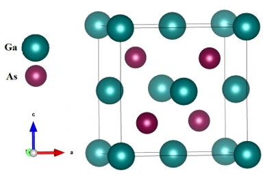
The structural optimization of GaAs in bulk, monolayer, and bilayer forms was performed using density functional theory (DFT). The optimized lattice constants for bulk GaAs are calculated to be a = 5.65 Å, which is in excellent agreement with the experimental value of a = 5.653 Å. This confirms that the computational method accurately models the bulk properties of GaAs (figure 1). The monolayer and bilayer GaAs were also optimized, with lattice constants slightly reduced compared to the bulk due to the absence of interlayer interactions in the monolayer and reduced interlayer bonding in the bilayer. These structural optimizations are essential for understanding the material's stability and are crucial for subsequent electronic property calculations.
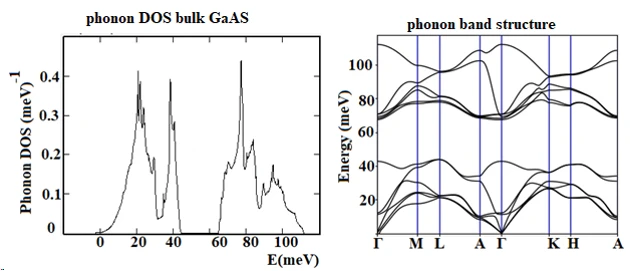
Figure 2. Calculated phonon band structure and phonon dencity of state for bulk structure of GaAs
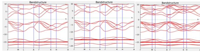
Next, we calculate the phonon dispersions for the bulk GaAs structures. The phonon band structure provides insight into the material’s vibrational modes, which directly influence thermal conductivity and electron-phonon interactions. For bulk GaAs, the phonon dispersion curves exhibit both acoustic and optical phonon branches, consistent with experimental data (figure 2). We now turn our focus to the electronic band structure of GaAs in its bulk, monolayer, and bilayer forms. The bulk GaAs structure exhibits an indirect bandgap of 1.42 eV, a hallmark of the bulk material, where the conduction band minimum (CBM) and the valence band maximum (VBM) are not aligned in momentum space (figure 3). This indirect transition is typical for GaAs and is responsible for its relatively lower optical efficiency compared to direct bandgap materials.
Upon transitioning to a monolayer, we observe a dramatic change: GaAs exhibits a direct bandgap of approximately 2.2 eV. This direct bandgap transition arises due to quantum confinement effects. As the material is reduced to the monolayer, the valence band maximum and conduction band minimum align at the Γ-point in the Brillouin zone, allowing for direct electronic transitions. This is a crucial property for optoelectronic applications, as direct bandgap materials exhibit higher efficiency in light emission and absorption, making monolayer GaAs highly suitable for LEDs, solar cells, and laser diodes. For the bilayer GaAs structure, the bandgap is slightly smaller than that of the monolayer, at approximately 2.1 eV, indicating that the quantum confinement effects are less pronounced in the bilayer compared to the monolayer. However, the bilayer still exhibits a direct bandgap, making it a promising candidate for optoelectronic devices that require slightly thicker materials but still benefit from the advantages of a direct transition. These results underscore the impact of dimensionality on the electronic properties of GaAs. The transition from bulk to monolayer and bilayer forms results in a shift from an indirect to a direct bandgap, significantly enhancing the optical efficiency of the material, particularly for applications requiring light emission and absorption in the visible and ultraviolet regions.
To explore the optical properties of GaAs, we calculate the real (ε₁(ω)) and imaginary (ε₂(ω)) components of the dielectric function for the bulk, monolayer, and bilayer structures (figure 4). The dielectric function provides critical information about how the material interacts with electromagnetic waves, particularly in the infrared and visible ranges, making it a key factor in determining the material's suitability for optoelectronic devices. For bulk GaAs, the dielectric function exhibits well-defined peaks in the imaginary component (ε₂(ω)), corresponding to indirect electronic transitions from the valence band maximum (VBM) to the conduction band minimum (CBM). These transitions occur at photon energies around 1.42 eV, consistent with the indirect bandgap of the material. As photon energy increases, the intensity of the absorption decreases significantly, particularly above the phonon absorption threshold around 5 eV. For the monolayer GaAs, the imaginary dielectric function (ε₂(ω)) exhibits sharper peaks at higher photon energies around 2.2 eV, corresponding to the direct bandgap transition. The real dielectric function (ε₁(ω)) for the monolayer shows a shift in the absorption edge compared to the bulk, indicating that the monolayer GaAs absorbs more efficiently at visible and ultraviolet photon energies, making it ideal for solar cell and LED applications. These results clearly highlight that monolayer GaAs offers significantly improved optical properties compared to bulk material, particularly in terms of photon absorption and light emission. For the bilayer GaAs, the absorption edge is similar to the monolayer, with a slight decrease in the intensity of the imaginary component. The bilayer structure still shows significant absorption in the visible range, though not as pronounced as in the monolayer. The optical transitions in the bilayer remain direct, and the material still exhibits high potential for optoelectronic devices, though the slightly smaller bandgap and reduced absorption might limit its performance in applications requiring extreme precision.The dielectric function results for both the monolayer and bilayer demonstrate the superior optical properties of reduced-dimensional GaAs, confirming its suitability for devices where high optical absorption and emission efficiency are paramount.
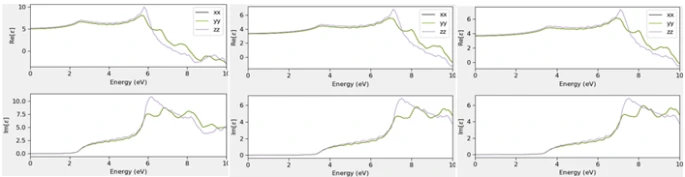
Figure 4. Calculated real and imaginary part of dielectric function of bulk bilayer and monolayer structure of GaAs
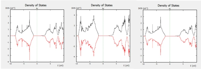
To gain a deeper understanding of the electronic structure of GaAs, we compute the density of states (DOS) for bulk, monolayer, and bilayer structures. The DOS reveals the distribution of electronic states across the material’s energy levels, providing insights into carrier transport and the electronic density at the valence and conduction bands. For bulk GaAs, the DOS is dominated by p-orbitals of As at the valence band maximum (VBM) and p-orbitals of Ga at the conduction band minimum (CBM). The monolayer GaAs shows a higher DOS at the CBM, indicating enhanced carrier transport due to the reduction in dimensionality. The monolayer GaAs also exhibits a higher density of states near the Fermi level, suggesting that the electron density in the monolayer will be more localized and responsive to external stimuli, such as electric fields, making it suitable for field-effect transistors (FETs) and photodetectors. The bilayer GaAs shows a DOS that is intermediate between the bulk and monolayer, with a lower density of states compared to the monolayer. This result suggests that the bilayer GaAs may offer a balanced trade-off between the optical performance of the monolayer and the electronic stability of the bulk, making it useful in electronic applications that require moderate carrier transport properties without the extreme confinement found in the monolayer.
In summary, the results from our density functional theory (DFT) simulations demonstrate the significant impact of dimensionality on the electronic, optical, and thermal properties of GaAs. The transition from bulk to monolayer and bilayer structures leads to a shift from an indirect bandgap to a direct bandgap, enhancing the material’s suitability for optoelectronic applications such as LEDs, solar cells, and laser diodes. Additionally, the dielectric function and density of states show enhanced absorption properties and increased electron mobility in the 2D forms, making monolayer GaAs particularly attractive for high-performance optoelectronic devices.
These findings underscore the importance of dimensionality in tailoring the material properties of GaAs, suggesting that 2D GaAs could be a game-changer for future nanoelectronics and optoelectronics. Future experimental investigations into dopant effects, mechanical stability, and device integration will be essential to fully realize the potential of GaAs in next-generation technologies.
1 X.H. Wang, L.W. Guo, H.Q. Jia, Z.G. Xing, Y. Wang, X.J. Pei, J.M. Zhou, H. Chen, Applied Physics Letters 94 (2009) 111913. https://doi.org/10.1063/1.3103559
2 X. Li, Z.S. Liu, D.G. Zhao, D.S. Jiang, P. Chen, J.J. Zhu, J. Yang, L.C. Le, W. Liu, X.G. He, X.J. Li, F. Liang, L.Q. Zhang, J.P. Liu, H. Yang, Y.T. Zhang, G.T. Du, Journal of Vacuum Science & Technology B 34 (2016) 041211. https://doi.org/10.1116/1.4950746
3 A.N. Jafarova, Modern Physics Letters B 38 (2024) 2350221. https://doi.org/10.1142/S0217984923502214
4 S.G. Asadullayeva, M.A. Mehrabova, A.N. Jafarova, A.S. Abiyev, Applied Physics Research 7(3) (2025) 264. https://doi.org/10.62476/apr.73264
5 W. Chikhaoui, J.M. Bluet, M.A. Poisson, N. Sarazin, C. Dua, C. Bru-Chevallier, Applied Physics Letters 96(7) (2010) 072107. https://doi.org/10.1063/1.3326079
6 N.A. Ismayilova, Z.A. Jahangirli, S.H. Jabarov, Journal of Superconductivity and Novel Magnetism 36 (2023) 1983. https://doi.org/10.1007/s10948-023-06641-1
7 N.A. Ismayilova, European Physical Journal Plus 139 (2024) 321. https://doi.org/10.1140/epjp/s13360-024-05122-1
8 N.A. Ismayilova, S.H. Jabarov, J.A. Guliyev, Ukrainian Journal of Physics 69 (2024) 754. https://doi.org/10.15407/ujpe69.10.754
9 N.A. Ismayilova, International Journal of Nanoscience 23 (2024) 2450006. https://doi.org/10.1142/S0219581X24500066
10 N.A. Ismayilova, Journal of Superconductivity and Novel Magnetism 38 (2025) 80. https://doi.org/10.1007/s10948-025-06920-z
11 S.G. Asadullayeva, Z.A. Jahangirli, M.A. Musayev, Q.Y. Eyyubov, A.S. Abiyev, Physics of the Solid State 67(6) (2025) 429. https://doi.org/10.1134/S1063783425601067
12 N. Ismayilova, A. Abiyev, Computational Condensed Matter 45 (2025) e01119. https://doi.org/10.1016/j.cocom.2025.e01119
13 S. Ganguly, A. Konar, Z.Y. Hu, H.L. Xing, D. Jena, Applied Physics Letters 101 (2012) 253519. https://doi.org/10.1063/1.4773244
14 B. Auld, Acoustic Fields and Waves in Solids, John Wiley & Sons, New York (1973).
15 Y.Y. Liu, B.L. Li, S.Z. Chen, X. Jiang, K.Q. Chen, Applied Physics Letters 111 (2017) 133107. https://doi.org/10.1063/1.4999127
16 Y.Y. Liu, Y.J. Zeng, P.Z. Jia, X.H. Cao, X. Jiang, K.Q. Chen, Journal of Physics: Condensed Matter 30 (2018) 275701. https://doi.org/10.1088/1361-648X/aac7f5
17 S.G. Asadullayeva, N.A. Ismayilova, Solid State Communications 394 (2024) 115725. https://doi.org/10.1016/j.ssc.2024.115725
18 C.R. Ryder, J.D. Wood, S.A. Wells, Y. Yang, D. Jariwala, T.J. Marks, G.C. Schatz, M.C. Hersam, Nature Chemistry 8(6) (2016) 597. https://doi.org/10.1038/nchem.2505
19 Y. Wang, W.-X. Zhou, L. Huang, C. Xia, L.-M. Tang, H.-X. Deng, L. Yongtao, K.-Q. Chen, J. Li, Z. Wei, 2D Materials 4 (2017) 025097. https://doi.org/10.1088/2053-1583/aa6efd?urlappend=%3Futm_source%3Dresearchgate.net%26utm_medium%3Darticle
20 S. Deng, L. Li, M. Li, Physica E 101 (2018) 44. https://doi.org/10.1016/j.physe.2018.03.016
21 J. Li, H. Liu, Journal of Materials Science 53 (2018) 15986.
22 R. González, W. López-Pérez, Á. González-García, M.G. Moreno-Armenta, R. González-Hernández, Applied Surface Science 433 (2018) 1049. https://doi.org/10.1016/j.apsusc.2017.10.136
23 S.G. Asadullayeva, Z.A. Jahangirli, T.G. Naghiyev, A.S. Abiyev, Current Applied Physics 76 (2025) 39. https://doi.org/10.1016/j.cap.2025.05.007
24 J. Tian, L. Liu, S. Xia, Y. Diao, F. Lu, Physics Letters A 383 (2019) 3018. https://doi.org/10.1016/j.physleta.2019.06.007
25 A.N. Jafarova, Modern Physics Letters B 37(26) (2023) 2350081. https://doi.org/10.1142/S0217984923500811
26 S.G. Asadullayeva, R.A. Ahmedov, A.A. Hadieva, V.K. Sarijanova, G.M. Fatullayeva, UNEC J. Eng. Appl. Sci. 3(2) (2023) 66. https://doi.org/10.61640/ujeas.2023.1209
27 S.G. Asadullayeva, Z.A. Jahangirli, European Physical Journal B 98 (2025) 142. https://doi.org/10.1140/epjb/s10051-025-00990-7
28 N.A. Ismayilova, A.S. Abiyev, Indian Journal of Physics 99 (2025) 5039. https://doi.org/10.1007/s12648-025-03685-y
Kh.O. Sadig, Sh.N. Aliyeva, Sh.R. Mammadova, Dimensionality-dependent electronic and optical properties of gaas: A density functional theory study of bulk, monolayer, and bilayer structures , UNEC J. Eng. Appl. Sci. 5(2) (2025) 110-115. https://doi.org/10.61640/ujeas.2025.1210
Anyone you share the following link with will be able to read this content:
This article is licensed under the Creative Commons Attribution ( CC BY 4.0 ) License, which permits unrestricted use, distribution, and reproduction in any medium, provided the original author and source are credited.
X.H. Wang, L.W. Guo, H.Q. Jia, Z.G. Xing, Y. Wang, X.J. Pei, J.M. Zhou, H. Chen, Applied Physics Letters 94 (2009) 111913. https://doi.org/10.1063/1.3103559
X. Li, Z.S. Liu, D.G. Zhao, D.S. Jiang, P. Chen, J.J. Zhu, J. Yang, L.C. Le, W. Liu, X.G. He, X.J. Li, F. Liang, L.Q. Zhang, J.P. Liu, H. Yang, Y.T. Zhang, G.T. Du, Journal of Vacuum Science & Technology B 34 (2016) 041211. https://doi.org/10.1116/1.4950746
A.N. Jafarova, Modern Physics Letters B 38 (2024) 2350221. https://doi.org/10.1142/S0217984923502214
S.G. Asadullayeva, M.A. Mehrabova, A.N. Jafarova, A.S. Abiyev, Applied Physics Research 7(3) (2025) 264. https://doi.org/10.62476/apr.73264
W. Chikhaoui, J.M. Bluet, M.A. Poisson, N. Sarazin, C. Dua, C. Bru-Chevallier, Applied Physics Letters 96(7) (2010) 072107. https://doi.org/10.1063/1.3326079
N.A. Ismayilova, Z.A. Jahangirli, S.H. Jabarov, Journal of Superconductivity and Novel Magnetism 36 (2023) 1983. https://doi.org/10.1007/s10948-023-06641-1
N.A. Ismayilova, European Physical Journal Plus 139 (2024) 321. https://doi.org/10.1140/epjp/s13360-024-05122-1
N.A. Ismayilova, S.H. Jabarov, J.A. Guliyev, Ukrainian Journal of Physics 69 (2024) 754. https://doi.org/10.15407/ujpe69.10.754
N.A. Ismayilova, International Journal of Nanoscience 23 (2024) 2450006. https://doi.org/10.1142/S0219581X24500066
N.A. Ismayilova, Journal of Superconductivity and Novel Magnetism 38 (2025) 80. https://doi.org/10.1007/s10948-025-06920-z
S.G. Asadullayeva, Z.A. Jahangirli, M.A. Musayev, Q.Y. Eyyubov, A.S. Abiyev, Physics of the Solid State 67(6) (2025) 429. https://doi.org/10.1134/S1063783425601067
N. Ismayilova, A. Abiyev, Computational Condensed Matter 45 (2025) e01119. https://doi.org/10.1016/j.cocom.2025.e01119
S. Ganguly, A. Konar, Z.Y. Hu, H.L. Xing, D. Jena, Applied Physics Letters 101 (2012) 253519. https://doi.org/10.1063/1.4773244
B. Auld, Acoustic Fields and Waves in Solids, John Wiley & Sons, New York (1973).
Y.Y. Liu, B.L. Li, S.Z. Chen, X. Jiang, K.Q. Chen, Applied Physics Letters 111 (2017) 133107. https://doi.org/10.1063/1.4999127
Y.Y. Liu, Y.J. Zeng, P.Z. Jia, X.H. Cao, X. Jiang, K.Q. Chen, Journal of Physics: Condensed Matter 30 (2018) 275701. https://doi.org/10.1088/1361-648X/aac7f5
S.G. Asadullayeva, N.A. Ismayilova, Solid State Communications 394 (2024) 115725. https://doi.org/10.1016/j.ssc.2024.115725
C.R. Ryder, J.D. Wood, S.A. Wells, Y. Yang, D. Jariwala, T.J. Marks, G.C. Schatz, M.C. Hersam, Nature Chemistry 8(6) (2016) 597. https://doi.org/10.1038/nchem.2505
Y. Wang, W.-X. Zhou, L. Huang, C. Xia, L.-M. Tang, H.-X. Deng, L. Yongtao, K.-Q. Chen, J. Li, Z. Wei, 2D Materials 4 (2017) 025097. https://doi.org/10.1088/2053-1583/aa6efd?urlappend=%3Futm_source%3Dresearchgate.net%26utm_medium%3Darticle
S. Deng, L. Li, M. Li, Physica E 101 (2018) 44. https://doi.org/10.1016/j.physe.2018.03.016
J. Li, H. Liu, Journal of Materials Science 53 (2018) 15986.
R. González, W. López-Pérez, Á. González-García, M.G. Moreno-Armenta, R. González-Hernández, Applied Surface Science 433 (2018) 1049. https://doi.org/10.1016/j.apsusc.2017.10.136
S.G. Asadullayeva, Z.A. Jahangirli, T.G. Naghiyev, A.S. Abiyev, Current Applied Physics 76 (2025) 39. https://doi.org/10.1016/j.cap.2025.05.007
J. Tian, L. Liu, S. Xia, Y. Diao, F. Lu, Physics Letters A 383 (2019) 3018. https://doi.org/10.1016/j.physleta.2019.06.007
A.N. Jafarova, Modern Physics Letters B 37(26) (2023) 2350081. https://doi.org/10.1142/S0217984923500811
S.G. Asadullayeva, R.A. Ahmedov, A.A. Hadieva, V.K. Sarijanova, G.M. Fatullayeva, UNEC J. Eng. Appl. Sci. 3(2) (2023) 66. https://doi.org/10.61640/ujeas.2023.1209
S.G. Asadullayeva, Z.A. Jahangirli, European Physical Journal B 98 (2025) 142. https://doi.org/10.1140/epjb/s10051-025-00990-7
N.A. Ismayilova, A.S. Abiyev, Indian Journal of Physics 99 (2025) 5039. https://doi.org/10.1007/s12648-025-03685-y