UNEC Journal of Engineering and Applied Sciences Volume 3, No 2, pages 54-60 (2023) Cite this article, ![]() 1588 https://doi.org/10.61640/ujeas.2023.1207
1588 https://doi.org/10.61640/ujeas.2023.1207
Semiconductor nanostructures are promising materials for future electronic and photonic devices. Nanostructures based on layered semiconductors such as GaSe (GaS, InSe, GaTe) are of particular interest for applications in optoelectronics, nonlinear optics, solar cells, LEDs and X-ray detectors [1-4]. Along with these, GaSe has two main advantages over other semiconductors (GaAs, CdS, CdSe, etc.): the large exciton binding energy (19.5 meV at 300 K) and the possibility of van der Waals homo- and heteroepitaxy for strongly lattice mismatched systems [5]. The reduced dimensionality of these compounds has a strong influence on the electronic, optical and nonlinear properties of the material. The strong bonding within the layers is considered to be covalent with some ionic contribution [6, 7]. At the same time, the interlayer bonding is much weaker and is mainly of van der Waals type. Because of this, easy splitting occurs parallel to the layers (perpendicular to the direction of the optical axis c) into plane-parallel plates with mirror-like surfaces. The hierarchy of weak forces and the ability of these materials to split easily, together with the low density of electronic states on freshly splitted surfaces (not exceeding ~1010 cm¯²) GaSe is an indirect bandgap semiconductor with a direct bandgap of 2.02 eV. The difference between the direct and indirect forbidden zone is quite small, about 25 meV.
Various GaSe nanostructures are known to be successfully synthesized. Methods of chemical vapor deposition of organometallic compounds and ultrasonic treatment of GaSe, laser ablation [1, 2] were used to obtain nanoparticles of this compound. Disc-shaped gallium selenide quantum dots were synthesized by the reaction of an organometallic compound (GaMe3) with trioctylphosphinselenium in a high-temperature solution of trioctylphosphine and trioctylphosphinoxide [3, 4]. It was shown that these particles, unlike spherical quantum dots with passivated surfaces, can strongly interact with each other. Laser ablation of the target in background argon gas, condenses the laser-generated plume, leading to the formation of metastable nanoparticles in the gas phase. Deposition of these nanoparticles on the substrate leads to the formation of nanoparticle ensembles, which are then post-processed to crystallize or sinter the nanoparticles.
GaSe crystals are promising as сonverters of nonlinear optics in the mid- and far-infrared ranges. However, it is difficult to increase the transmittance of the GaSe surface up to 77% using conventional brightening coatings due to poor surface quality, which leads to coating adhesion problems. Anti-reflection microstructures (ARM) offer an alternative way to increase the surface transmittance. In [4-6], ARM were fabricated on GaSe wafer surface by single-pulse femtosecond laser ablation. An average GaSe surface transmittance of 94 % in the range of 7-11 m and a maximum transmittance of 97.8 % at 8.5 m were obtained. The proposed method can be used to improve the efficiency of GaSe-based nonlinear transducers [7].
Previously, we reported the formation of GaSe nanoparticles in solution obtained by laser ablation of a solid target in a liquid medium. Laser ablation of nanoparticles in liquid has caused great interest due to its simplicity, lack of the need for surfactants, and good control over the size and shape of the synthesized nanoparticles [8, 9]. In this method, many parameters such as laser flux density, laser wavelength, pulse duration and type of colloidal solution can affect the characteristics of the synthesized nanoparticles.
It should be noted that during laser ablation, bulk GaSe crystals grown by the Bridgman method were used as target materials. Laser ablation was performed either in vacuum or by immersing the target in various liquids, using ultra-short laser pulses, nano and femtosecond durations. Indeed, synthesizing GaSe nanoparticles by laser ablation, as mentioned above, has great advantages over other methods. However, it should be considered that this method requires the growth of unalloyed GaSe crystals, which is by no means a simple technological task. On the other hand, the purity of the used crystals for the preparation of nanostructures is very important.
In this work, we propose a slightly different way of obtaining GaSe nanoparticles, namely, by direct interaction of laser radiation with Ga element and SeO2 solution. As shown by our experimental studies, the structural characteristics and optical properties of GaSe nanoparticles significantly exceed the similar characteristics of nanoparticles obtained by other methods.
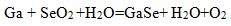
GaSe nanoparticles were synthesized by laser ablation of a solid target in a liquid medium. Special pure Ga (99%) in SeO2 solution was used as the initial raw material. The reaction proceeded according to the following formula:
Immediately after irradiation by laser pulse, GaSe nanoparticles were formed. The ablation process was carried out by laser radiation with the wavelength λ=1064 nm, with pulse energy 135 mJ and ablation time ~ 10 min. A pulsed Nd:YAG-laser with built-in generators of the 2nd and 3rd harmonics was used as a radiation source to generate radiation with wavelengths of 1064, 532 and 335 nm. The laser pulse duration was 10 ns with a maximum power of ~12 MW/cm². The intensity of the radiation was varied using calibrated neutral light filters. Optical absorption and luminescence spectra of GaSe nanoparticles were investigated using an automatic M833 double-dispersion monochromator (spectral resolution ~0.024 nm at a wavelength of 600 nm), with computer control and a detector recording radiation in the wavelength range 350-2000 nm.
The scheme of the experimental setup is presented in figure 1. Laser radiation with wavelength 1064 nm, focused by a positive lens (f=11 cm), was used for ablation of GaSe nanoparticles. Laser ablation of GaSe crystal, was carried out in a quartz cuvette containing Ga element and 5 ml of SeO2 solution without adding any surfactants. The ablation process was carried out by laser radiation with wavelength λ=1064 nm, with pulse energy 135 mJ for ~ 10 min.
The color of a fresh suspension of colloidal GaSe was found to depend on the laser radiation flux density. For GaSe nanoparticles synthesized at low laser flux density, the color was light red, which changed to dark orange after increasing the laser flux density.
Figure 1. Schematic diagram of the experimental setup for ablation of GaSe nanoparticles
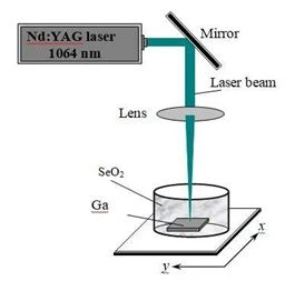
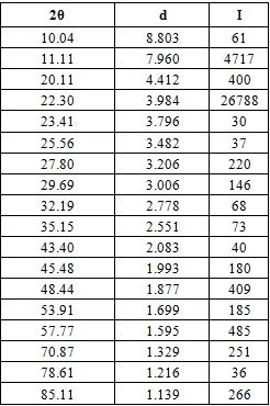
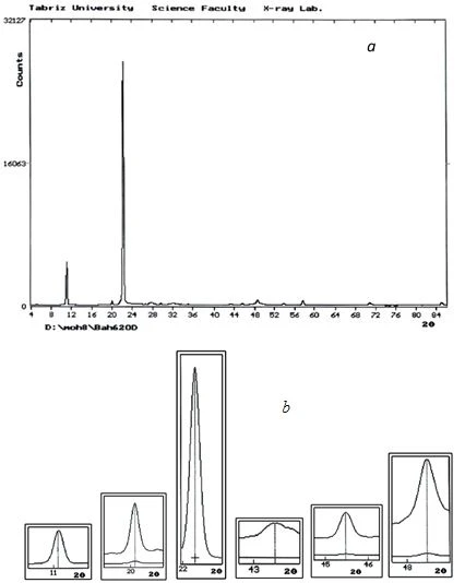
Figure 2,a and b show the X-ray diffractograms (XRD) of nanoparticles from GaSe colloidal solution droplets dried on a clean glass substrate. CuKα, λ=1.544178 A0 SSFOM: F17-610.0.5.10.60 were used as an emission source. The table shows the diffraction angles (2θ), diffraction plane spacing (d) and line intensities (I) observed in the GaSe diffractogram.
The X-ray diffraction patterns show that the synthesized GaSe nanoparticles have the same hexagonal structure as the bulk material.
On the basis of the X-ray diffractogram, the dimensions of the obtained nanoparticles were calculated using the Debye-Scherrer formula [11]:

where D is the size of nanoparticles, k = 0.9 is the line shape factor, β = 0.035 А0 is the half width at maximum intensity (FWHM- Full Width at Half Maximum), λ is the wavelength of X-ray radiation (λ=1.54 А0), θ is the Bregge angle (cos =0,727).
The evaluation shows the formation of nanoparticles with diameters ranging from 2 to 25 nm was observed in the colloidal solution.
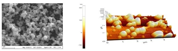
Scanning Electron Microscope (SEM), Atomic Force Microscope (AFM) and Energy Dispersive X-ray Energy Dispersive Spectroscopy (EDAX) were used to investigate the internal structure of GaSe nanoparticles.
Figure 2. a) Diffractogram (XRD) of GaSe nanoparticles on glass substrate, b) Diffractogram of individual lines of GaSe nanoparticles
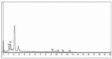
SEM images show that the obtained substances consist of spherical nanocrystals with sizes of 2-25 nm, which are assembled in a polydispersive form (Figure 3,a). Figure 3,b shows the AFM images of the nanoparticles GaSe on a glass substrate. As can be seen from the figures, no homogeneous distribution of particles is observed in the presented figures. The EDAX method shows that the ratio of gallium to selenium is in Ga : Se = 1:1, showing that the composition of matter is in stoichiometric ratio (Figure 4).
Figure 5,a shows the photoluminescence spectrum of GaSe nanoparticles, excited by the second harmonic of Nd:YAG laser ( eV). As can be seen from figure, the emission maximum of nanoparticles corresponds to the wavelength ~ 473 nm (2.62 eV). The half-width of the emission line is ~10 А°. This indicates that stimulated emission is observed in GaSe nanostructures under laser excitation. Comparison of luminescence spectra of GaSe nanoparticles obtained by direct interaction of laser radiation with Ga element and SeO2 solution with formation of GaSe nanoparticles in solution, obtained by laser ablation of solid target in liquid medium shows significant differences between these emission spectra (figure 5,b). In both cases the position of the emission line does not change and is of the order of ~ 473 nm. This suggests that the nature of the emission is the same in both cases. At the same laser light excitation intensities, the emission intensity is one order of magnitude higher than the emission intensity during laser ablation of GaSe solid target in liquid medium. Moreover, the half-width of the emission line at laser ablation of GaSe solid target is much higher (~25 times) than the half-width of the emission line at formation of nanoparticles by direct interaction of laser radiation with Ga element and SeO2 solution. In our opinion, this difference in the luminescence spectra of GaSe nanoparticles obtained by different methods is due to the fact that during the direct synthesis of nanoparticles by Ga element and SeO2 solution, there are no various types of imperfections (impurities, defects, etc.) inherent in semiconductor crystals during growth.
Figure 5. Photoluminescence spectra of GaSe nanoparticles obtained by direct interaction of laser radiation with Ga element and SeO2 solution (a) and with the formation of GaSe nanoparticles in solution obtained by laser ablation of solid target in liquid
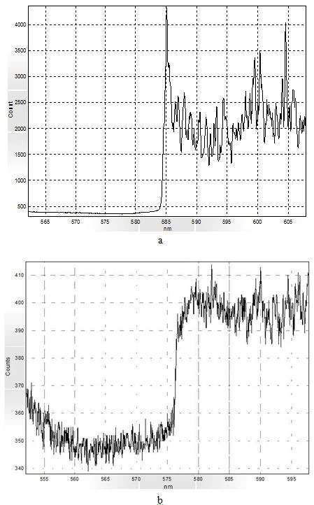
As for the nature of the observed emissions, we believe that they are due to radiative recombination of free excitons.
This is evidenced by the stability and rather significant narrowness of the line (of the order of a few angstroms). Knowing the emission maximum ( ~2.62 eV) and the energy of free excitons in GaSe (Efe~20 meV) we can determine the width of the forbidden zone of nanoparticles Eg=ω+E_fe which is equal to 2.64 eV. This value is 0.53 eV larger than the forbidden band width of bulk unalloyed GaSe crystal ( Eg = 2.11 eV).
GaSe nanoparticles were obtained by direct interaction of laser radiation with Ga element and SeO2 solution. Under these ablation conditions in colloidal solution, the formation of nanoparticles with diameter from 2 to 25 nm was observed. It is shown that the synthesized nanoparticles retain the crystalline structure of bulk material and emit photoluminescence at 473 nm associated with radiative recombination of free excitons. Comparison of luminescence spectra of GaSe nanoparticles obtained by direct interaction of laser radiation with element Ga and SeO2 solution with the formation of GaSe nanoparticles in solution, obtained by laser ablation of a solid target in a liquid medium shows significant differences between these emission spectra.
1 S.L. Stoll, E.G. Gillan, A.R. Barron, Chemical Vapor Deposition 2(5) (1996) 182. https://doi.org/10.1002/cvde.19960020506
2 K. Allakhverdiev, J. Hagen, Z. Salaeva, Physica Status Solidi (A) 163(1) (1997) 121. https://doi.org/10.1002/1521-396X(199709)163:1%3C121::AID-PSSA121%3E3.0.CO;2-K
3 D.V. Rybkovskiy, A.V. Osadchy, E.D. Obraztsova, Journal of Nanoelectronics and Optoelectronics 8(1) (2013) 110. https://doi.org/10.1166/jno.2013.1430
4 S. Elafandi, Z. Ahmadi, N. Azam, M. Mahjouri-Samani, Nanomaterials 10(5) (2020) 908. https://doi.org/10.3390/nano10050908
5 V. Chikan, D.F. Kelley, Nano Letters 2(2) (2002) 141. https://doi.org/10.1021/nl015641m
6 N.G. Semaltianos, Critical reviews in Solid State and Materials Sciences 35 (2010) 105. https://doi.org/10.1080/10408431003788233
7 A.A. Bushunov, A.A. Teslenko, M.K. Tarabrin, V.A. Lazarev, L.I. Isaenko, A.P. Eliseev, S.I. Lobanov, Optics Letters 45(21) (2020) 5994. https://doi.org/10.1364/OL.404515
8 M.A. Jafarov, V.M. Salmanov, A.G. Guseinov, G.B. Ibragimov, R.M. Mamedov, T.A. Mamedova, F.Sh. Akhmedova, AJP Fizika XXIX(3) (2023) 13.
9 H.L. Zhuang, R. G. Hennig, Chem. Mater. 25(15) (2013) 3232. https://doi.org/10.1021/cm401661x
10 A.G. Kyazym-zadea, M. Karabulurb, A.Kh. Dincherb, V.M. Salmanova, M.A. Dzhafarova, A.M. Guseinova, and R.M. Mamedova, Nanotechnologies in Russia 10 (2015) 794. https://doi.org/10.1134/S1995078015050122
11 S. Samuel, International Journal of Nanotechnology 1(1/2) (2004) 42. https://dx.doi.org/10.1504/IJNT.2004.003712
12 A.S. Abdinov, R.F. Babaeva, R.M. Rzaev, Inorganic Materials 48 (2012) 781.
13 A.S. Abdinov, R.F. Babayeva, S.I. Amirova et al., Semiconductors 48 (2014) 981.
M.A. Jafarov, V.M. Salmanov, A.H. Huseynov, R.M. Mamedov, T.A. Mamedova, F.S. Ahmedova, A.B. Aliyeva, GaSe nanoparticles synthesized by laser ablation method, UNEC J. Eng. Appl. Sci. 3(2) (2023) 54-60 https://doi.org/10.61640/ujeas.2023.1207
Anyone you share the following link with will be able to read this content:
This article is licensed under the Creative Commons Attribution ( CC BY 4.0 ) License, which permits unrestricted use, distribution, and reproduction in any medium, provided the original author and source are credited.
S.L. Stoll, E.G. Gillan, A.R. Barron, Chemical Vapor Deposition 2(5) (1996) 182. https://doi.org/10.1002/cvde.19960020506
K. Allakhverdiev, J. Hagen, Z. Salaeva, Physica Status Solidi (A) 163(1) (1997) 121. https://doi.org/10.1002/1521-396X(199709)163:1%3C121::AID-PSSA121%3E3.0.CO;2-K
D.V. Rybkovskiy, A.V. Osadchy, E.D. Obraztsova, Journal of Nanoelectronics and Optoelectronics 8(1) (2013) 110. https://doi.org/10.1166/jno.2013.1430
S. Elafandi, Z. Ahmadi, N. Azam, M. Mahjouri-Samani, Nanomaterials 10(5) (2020) 908. https://doi.org/10.3390/nano10050908
V. Chikan, D.F. Kelley, Nano Letters 2(2) (2002) 141. https://doi.org/10.1021/nl015641m
N.G. Semaltianos, Critical reviews in Solid State and Materials Sciences 35 (2010) 105. https://doi.org/10.1080/10408431003788233
A.A. Bushunov, A.A. Teslenko, M.K. Tarabrin, V.A. Lazarev, L.I. Isaenko, A.P. Eliseev, S.I. Lobanov, Optics Letters 45(21) (2020) 5994. https://doi.org/10.1364/OL.404515
M.A. Jafarov, V.M. Salmanov, A.G. Guseinov, G.B. Ibragimov, R.M. Mamedov, T.A. Mamedova, F.Sh. Akhmedova, AJP Fizika XXIX(3) (2023) 13.
H.L. Zhuang, R. G. Hennig, Chem. Mater. 25(15) (2013) 3232. https://doi.org/10.1021/cm401661x
A.G. Kyazym-zadea, M. Karabulurb, A.Kh. Dincherb, V.M. Salmanova, M.A. Dzhafarova, A.M. Guseinova, and R.M. Mamedova, Nanotechnologies in Russia 10 (2015) 794. https://doi.org/10.1134/S1995078015050122
S. Samuel, International Journal of Nanotechnology 1(1/2) (2004) 42. https://dx.doi.org/10.1504/IJNT.2004.003712
A.S. Abdinov, R.F. Babaeva, R.M. Rzaev, Inorganic Materials 48 (2012) 781.
A.S. Abdinov, R.F. Babayeva, S.I. Amirova et al., Semiconductors 48 (2014) 981.