UNEC Journal of Engineering and Applied Sciences Volume 3, No 1, pages 5-9 (2023) Cite this article, ![]() 2023 https://doi.org/10.61640/ujeas.2023.0501
2023 https://doi.org/10.61640/ujeas.2023.0501
Single crystals of p-GaSe with their diverse photoelectric properties and unique prospects for practical application in optoelectronics have attracted the attention of researchers from various countries of the world for many years [1–11]. However, to date, no systematic study of the features and mechanisms of the dependence of the relaxation processes (kinetics) of the intrinsic photoconductivity of this semiconductor on various factors has been carried out. Taking into account that the nature of the photoconductivity kinetics plays an important role in the operation of photoelectric devices and its study is also one of the powerful methods for studying the mechanism of generation-recombination processes in semiconductors [12, 13], the aim of this work was to experimentally reveal the features of relaxation processes (kinetics) intrinsic photoconductivity and elucidate their mechanism in single crystals of the p-GaSe layered semiconductor.
The measurements were carried out using an experimental setup assembled on the basis of an MDR-12 monochromator [14] at temperatures Т=77÷300 K, electric field strengths E=5.0•101÷3.0∙103 V∕cm applied to the test sample, light intensities Ф=1 101÷5 102 Lk, respectively, on samples of specially undoped (pure) p-GaSe crystals with different initial (having at T=77 K) dark resistivity (ρD0≈1 104 ÷ 8 107 Ω∙cm).
Having the shape of a rectangular parallelepiped with a thickness of ~0.150÷0.300 mm and transverse dimensions of ~3.00÷5.00 mm in the directions perpendicular to and along the (001) plane of the crystal [15], respectively, the samples were obtained by simple mechanical separation from a large single-crystal p-GaSe ingot grown by a modified Bridgman method [2]. Metallic indium served as the material for the current contacts. In all measurements, the light beam incident on the sample was directed perpendicularly, and the current through the sample, depending on the location of the current contacts, was directed perpendicularly or along the (001) plane of the crystal.
It has been established that in the low-temperature region (at T≤250 K), the behavior of the photoconductivity kinetics (dependence of the photoconductivity on time) in p-GaSe crystals, in addition to temperature (T), also significantly depends on the strength of the applied electric field (E) and the initial (having at 77 K) the value of the dark resistivity (ρD0) of the test sample.
Figure 1. Kinetics of photoconductivity in low-resistance (curves 1 and 2) and high-resistance (curves 3 and 4) p-GaSe crystals at various electric field strengths in the low-temperature region
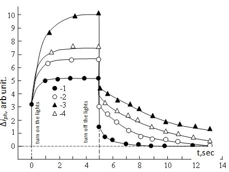
ρD0, Ω∙cm: 1, 2 - 1∙104; 3, 4 - 8∙107
T=77 K, λo=0.58 µm, Фo/Фmo=0.6, E, V∕cm: 1, 3 - 1.2 10², 2, 4 - 2 10³
In samples with ρD0<2⋅105 Ω∙cm in the temperature range Т≤150 K at electric fields corresponding to the linear section of the static dark CVC [16], both the processes of establishing a stationary value and the disappearance of photoconductivity upon turning on and off the illumination, respectively, are determined time constant (τ), equal in value to the lifetime of nonequilibrium charge carriers (τ0≈10-7÷10-6 s depending on T) in the semiconductor under study [17] (Figure 1, curve 1). With a subsequent increase in the electric field strength: firstly, on both (both on the front and on the rear) shoulders of the photocurrent pulse behind the fast (with a characteristic time τ=τ0≈10-7÷10-6 s), a relatively slow a section, the value of the characteristic time of which changes with the change in E, and in some cases at 77 K reaches up to seconds (Figure 1, curve 2); secondly, the total rise time (τr≈10-4÷10-3 s) and decay time (τd≈10-2÷10-1 s) of photoconductivity differ by several orders of magnitude. At electric field strengths E≥E1-2, where E1-2 is the value of the electric field strength corresponding to the transition of the static dark CVC from the initial linear section to the first quadratic one [16], with an increase in E, the value of photoconductivity also increases markedly compared to that at E<E1-2.
Under the same external conditions in samples with ρD0≥6•104 Ω∙cm, the situation noticeably differs from that in samples with ρD0<2•105 Ω∙cm. In particular, at Е<Е1-2 (Figure 1, curve 3) and Т≤140÷150 K (depending on the value of ρD0), the processes of establishing a stationary value and the disappearance of photoconductivity consist not of two, but of three successive stages: the initial one is fast, the next one is relatively slow, and finally the third one is slow. The first two stages do not differ in the nature of their course from those taking place in samples with ρD0<2•105 Ω∙cm (Figure 1, curve 1), but the third one has a different character. In particular, this stage of the photoconductivity kinetics is slowly relaxing [18], the characteristic time for it itself turns out to be time dependent - it increases during relaxation and, in this case, residual photoconductivity (irp) is observed [5, 18]. At low illumination, starting from the strength of the electric field applied to the sample under study, corresponding to the transition from the first quadratic region to the region of a sharp increase in the dark static CVC [16], the duration of the third growth region (Figure 1, curve 4), the values of the total and residual photoconductivities, the duration the third - the final stage of the disappearance of photoconductivity, also decrease. At higher values of the electric field applied to the test sample in high-resistance crystals, the process of photoconductivity decay accelerates sharply - the residual photoconductivity is electrically erased and the erasing effect of individual successive short-term electrical pulses is added. The erasing effect of the electric field is reversible - with a decrease in E to E<E1-2, the residual conductivity is restored again.
The dependence of the photoconductivity kinetics on temperature mainly consists in the fact that the difference between the photoconductivity kinetics of high-resistance and low-resistance crystals found at E<E1-2 gradually decreases with increasing temperature and the situation approaches that which occurs in the most low-resistance crystals.
Statistical analysis of the experimental results obtained allows us to state that, regardless of the value of ρD0, all p-GaSe crystals under study contain both attractive and repulsive trapping centers. In low-resistance crystals under all the conditions considered, as well as at high temperatures in all the crystals under study, the initial sharp increase and decrease in photoconductivity are associated with the predominance of monomolecular recombination and the direct recombination of nonequilibrium holes through fast s-recombination centers, respectively, and the slow components of photoconductivity relaxation are due to the inclusion of their generation-recombination processes are also successive phenomena of capture and release by attachment centers [12]. At low values of the electric field strength, the capture of the main charge carriers by the attractive capture centers dominates. With an increase in E –, their capture also begins to appear on repulsive centers [12, 13].
In high-resistance p-GaSe crystals, in contrast to low-resistance ones, in addition to attractive and repulsive trapping centers, there are also random macroscopic defects (RMD) [19], which have a much greater effect on the photoconductivity of the samples under study [5]. In this case, the photoconductivity as a whole consists of the concentration component and the mobility component associated with the light straightening of the drift barriers [20]. Due to the exponential nature [20], under certain conditions, the latter can be significant. The dependence of the value of drift barriers on the action of light, first of all, manifests itself in the value of the photocurrent, as well as in the third segment of the kinetics of its leading and trailing edges. The presence of recombination barriers - causes residual conductivity [5].
The revealed features of the influence of an electric field with a higher strength on the kinetics of photoconductivity in high-resistance p-GaSe crystals, in addition to the capture and release of nonequilibrium charge carriers by attracting and repulsive centers, are also due to the injection (electrical) straightening of the fluctuations of the electronic potential [21] - the electrical erasure of the residual photoconductivity [five]. In particular, the charge carriers injected into the sample lead to an effect similar to optical straightening, i.e., “injection straightening” of drift barriers, which correspondingly accompanies an increase in the dark conductivity of the sample under study. Due to partial compensation of the SMD space charge by injected charge carriers [22], the height of recombination barriers also decreases, which in turn leads to electrical erasure of the residual photoconductivity.
Thus, we can conclude that in the crystals of the p-GaSe layered semiconductor:
- The kinetics of photoconductivity, in addition to temperature, light intensity, also significantly depends on the value of the initial dark resistivity (ρD0) of the sample under study and the strength of the electric field applied to it (E);
- The dependences of the photoconductivity kinetics on ρD0 and E can be explained within the framework of the model of a spatially inhomogeneous crystalline semiconductor, which has both attractive and repulsive trapping centers in the band gap;
- In low-resistance crystals, the formation of photoconductivity kinetics at low E is dominated by the processes of capture of non-equilibrium charge carriers on attracting centers, and at higher E - on repulsive capture centers;
- In high-resistivity crystals, in addition to attracting and repulsing centers, a significant role is also played by drift and recombination barriers due to the presence of random macroscopic defects, as well as injection, in the formation of the photoconductivity kinetics;
- Within the framework of a model that combines the presence of attractive and repulsive centers, as well as random macroscopic defects directly related to the layered crystal structure, it is possible to satisfactorily explain the features of the photoconductivity kinetics of the p-GaSe layered semiconductor.
1 R.H. Bube, E.L. Lind, Phys. Rev. 115(5) (1959) 1159
2 R.F. Mehtiev, G.B. Abdullaev, G.A. Akhundov, DAN Az. SSR. 1962. 18(6) 11.
3 G.B. Abdullaev, M.R. Akhundov, G.A. Akhundov, Phys. Stat. Solidi 16(1) (1966) 209.
4 B.H. Tredgold, R.H. Williams, A. Clark, Phys. Stat. Sol. 1970. Vol. 3(2) (1970) 407.
5 E.B. Borisenko, N.N. Kolesnikov, D.N. Borisenko, S.I. Bozhko, Journal of Crystal Growth 316(1) (2011) 20.
6 A.Sh. Abdinov, A.G. Kazim-zade, FTP 9(11) (1975) 2135.
7 A.Sh. Abdinov, Ya.G. Akperov, V.K. Mamedov, El.Yu. Salaev, FTP 14(4) (1980) 749.
8 A.Sh. Abdinov, V.K. Mamedov, El.Yu. Salaev, FTP 14(4) (1980) 754.
9 C.H. Ho, M.H. Hsieh, C.C. Wu, Review of Scientific Instruments 77(11) (2006) 113102.
10 V.V. Atuchin, Y.M. Andreev, K.A. Kokh, G.V. Lanskii, A.V. Shaiduko, T.I. Izaak, V.A. Svetlichnyi, Proceedings of SPIE 8772 (2013) 87721Q-3.
11 A.Sh. Abdinov, R.F. Babaeva, N.A. Ragimova, E.A. Rasulov, Applied Physics 6 (2016) 72.
12 S.M. Ryvkin, Photoelectric phenomena in semiconductors. M.: Nauka, 1963. 494 p.
13 L.E. Vorobyov, S.N. Danilov, G.G. Zegrya, D.A. Firsov, V.A. Shalygin, I.N. Yassievich, Beregulin E.V. Photoelectric phenomena in semiconductors and size-quantum structures. St. Petersburg: Nauka (2001) 248 p.
14 A.Sh. Abdinov, R.F. Babaeva, Inorganic Materials 55(8) (2019) 758.
15 Z.S. Medvedeva Chalcogenides of elements III B of the subgroup of the periodic system. M.: Nauka (1968) 216 p.
16 M. Lampert, P. Mark, Injection currents in solids. M.: Mir (1973) 416 p.
17 G.B. Abdullaev, M.Kh. Alieva, G.L. Belenkii, A.Z. Mamedova, Phys. Stat. Solidi 37(2) (1970) 571.
18 M.K. Sheinkman, A.Ya. Shik, FTP 10(2) (1976) 209.
19 A.Ya. Shik, Journal of Experimental and Theoretical Physics 15 (1972) 408.
20 A.G. Kazym-zade, M.M. Panahov, V.I. Tagirov, Letters to ZhTF. 1980. V. 6(17) (1980) 1040.
21 A.G. Kazym-zade, Ya.A. Bairamov, V.I. Tagirov, FTP 16(9) (1982) 1685.
22 B.I. Shklovsky, A.L. Efros, Electronic properties of doped semiconductors. M.: Science. (1979) 416 p.
R.F. Babayeva, A.Sh. Abdinov, S.I. Amirova, N.A. Ragimova, E.A. Rasulov, Relaxation features of own photoconductivity in p-GaSe single crystals, UNEC J. Eng. Appl. Sci. 3(1) (2023) 5-9 https://doi.org/10.61640/ujeas.2023.0501
Anyone you share the following link with will be able to read this content:
This article is licensed under the Creative Commons Attribution ( CC BY 4.0 ) License, which permits unrestricted use, distribution, and reproduction in any medium, provided the original author and source are credited.
R.H. Bube, E.L. Lind, Phys. Rev. 115(5) (1959) 1159
R.F. Mehtiev, G.B. Abdullaev, G.A. Akhundov, DAN Az. SSR. 1962. 18(6) 11.
G.B. Abdullaev, M.R. Akhundov, G.A. Akhundov, Phys. Stat. Solidi 16(1) (1966) 209.
B.H. Tredgold, R.H. Williams, A. Clark, Phys. Stat. Sol. 1970. Vol. 3(2) (1970) 407.
E.B. Borisenko, N.N. Kolesnikov, D.N. Borisenko, S.I. Bozhko, Journal of Crystal Growth 316(1) (2011) 20.
A.Sh. Abdinov, A.G. Kazim-zade, FTP 9(11) (1975) 2135.
A.Sh. Abdinov, Ya.G. Akperov, V.K. Mamedov, El.Yu. Salaev, FTP 14(4) (1980) 749.
A.Sh. Abdinov, V.K. Mamedov, El.Yu. Salaev, FTP 14(4) (1980) 754.
C.H. Ho, M.H. Hsieh, C.C. Wu, Review of Scientific Instruments 77(11) (2006) 113102.
V.V. Atuchin, Y.M. Andreev, K.A. Kokh, G.V. Lanskii, A.V. Shaiduko, T.I. Izaak, V.A. Svetlichnyi, Proceedings of SPIE 8772 (2013) 87721Q-3.
A.Sh. Abdinov, R.F. Babaeva, N.A. Ragimova, E.A. Rasulov, Applied Physics 6 (2016) 72.
S.M. Ryvkin, Photoelectric phenomena in semiconductors. M.: Nauka, 1963. 494 p.
L.E. Vorobyov, S.N. Danilov, G.G. Zegrya, D.A. Firsov, V.A. Shalygin, I.N. Yassievich, Beregulin E.V. Photoelectric phenomena in semiconductors and size-quantum structures. St. Petersburg: Nauka (2001) 248 p.
A.Sh. Abdinov, R.F. Babaeva, Inorganic Materials 55(8) (2019) 758.
Z.S. Medvedeva Chalcogenides of elements III B of the subgroup of the periodic system. M.: Nauka (1968) 216 p.
M. Lampert, P. Mark, Injection currents in solids. M.: Mir (1973) 416 p.
G.B. Abdullaev, M.Kh. Alieva, G.L. Belenkii, A.Z. Mamedova, Phys. Stat. Solidi 37(2) (1970) 571.
M.K. Sheinkman, A.Ya. Shik, FTP 10(2) (1976) 209.
A.Ya. Shik, Journal of Experimental and Theoretical Physics 15 (1972) 408.
A.G. Kazym-zade, M.M. Panahov, V.I. Tagirov, Letters to ZhTF. 1980. V. 6(17) (1980) 1040.
A.G. Kazym-zade, Ya.A. Bairamov, V.I. Tagirov, FTP 16(9) (1982) 1685.
B.I. Shklovsky, A.L. Efros, Electronic properties of doped semiconductors. M.: Science. (1979) 416 p.