UNEC Journal of Engineering and Applied Sciences Volume 2, No 2, pages 18-22 (2022) Cite this article, ![]() 1432
1432
The synthesis and characterization of semiconductor nanoparticles have attracted much interest because of their novel properties as a consequence of the large number of surface atoms and the three-dimensional confinement of the electrons [1-7]. Altering the size of the particles alters the degree of the confinement of the electrons and affects the electronic structure of the solid, especially the band gap edges. Among a variety of semiconductor materials, the binary metal chalcogenides of group II-VI have been extensively studied [1-6]. For example, nanocrystalline thin films of ZnS and CdS are attractive materials in photoconducting cells and optoelectronic devices such as solar cells and photodetectors [7-9].
Alloying of semiconductors is one of the simplest techniques used for tailoring the energy band gap, lattice parameter, electronic and optical properties generally in alloys; the lattice parameter varies linearly with composition and follows the Vegard’s law. Among the different ternary II-VI semi- conductors, ZnxCd1-xS has been widely used as a wide band gap material in heterojunction solar cells, photoconductive devices, high- density optical recording and for blue or even ultraviolet laser diodes.
In this paper, we report a novel chemical reduction route to synthesize ZnS, CdS and ZnxCd1-xS nanocrystals at room temperature.
Typically, an appropriate amount of sulfur powder was added to a flask containing 50 mL of tetrahydrofuran (THF). After being stirred using magnetic stirrer for 5 min, the mixture becomes a colorless transparent solution. A stoichiometric amount of ZnCl2 was added to the flask and a black suspension formed upon stirring. After the addition of NaBH4, the suspension turned light green. After the mixture was stirred for 3 h, a white precipitate formed. Then the precipitate was centrifuged and dried at room temperature. The sample is now ready for characterization. For the preparation of nanocrystalline CdS, the process was the same as above except that anhydrous CdCl2 was used instead of ZnCl2. For the preparation of ZnxCd1-xS stoichiometric anhydrous ZnCl2 and CdCl2 powders were used according to the molar ratios in the target compounds Zn0.7Cd0.3S, Zn0.5Cd0.5S. The X-ray powder diffraction (XRD) was obtained using a Rigaku MiniFlex-II X-ray Diffractometer using CuKα radiation. Transmission electron microscope (TEM) images were obtained using the JEOL JEM-200 TEM operated at 200 kV. UV- VIS absorption spectra were recorded using a Shimadzu Pharmaspec-1700 spectrophotometer with a 1-cm quartz cell at room temperature. Colloid solutions in ethanol were prepared ultrasonically for the UV-VIS and the photoluminescence (PL) measurements. The Photoluminescence of ZnS, CdS and ZnxCd1-xS nanoparticles were measured using Perkin Elmer LS 55 Fluorescence Spectrometer.
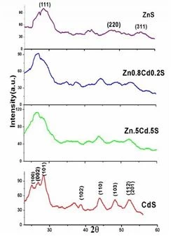
Figure 1 shows the x-ray diffraction peaks of the as prepared ZnS, CdS and different ZnxCd1-xS samples. Samples are taken in the powder form and the measured angle is within 20-60 degree. Results show well defined peaks in each case and the peak positions gradually change with composition of the samples. All XRD patterns show obvious size broadening effect. In case of CdS the half width of the first peak is maximum indicating that particle size is minimum which is also confirmed by TEM pattern. For CdS the XRD pattern can be indexed as a wurtzite phase structure with strongly characteristic (100), (002), (101), (102), (110), (103) and (112) peaks, while for ZnS XRD pattern mainly reflects its zincblende character [(111), (220) and (311) peaks] with some wurtzite character [such as the exixtence of a vague (103)], which indicates either that the ZnS particles have a zincblende structure with some wurtzite stacking faults or that most particles have a zincblende structure with others having a wurtzite structure. As for the ZnxCd1-xS nanocrystals the diffraction peaks in the XRD patterns gradually shift to larger angels and a phase transition from wurtzite to zincblende occurs with an increase of Zn content. This continuous peak shifting of the nanocrystals also indicates that there is no phase separation or separated nucleation of ZnS or CdS in the ZnxCd1-xS nanocrystals.
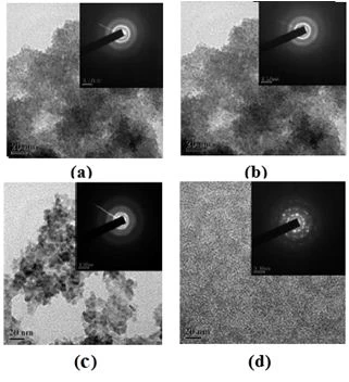
Samples are well dispersed in ethanol by ultra sonification and it is placed on the carbon coated grid for TEM measurement. Figure 2 (a, b, c, d) shows TEM pattern of the as prepared samples. The particle size is measured in each case from the photograph.
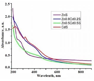
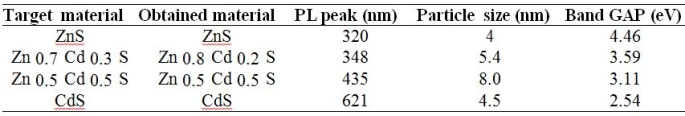
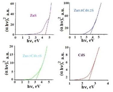
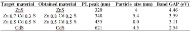
TEM analysis indicates that the particles are in the nano range for different samples. Particle size for ZnS is found to be 4 nm. Particle size gradually increases with increase of Cd content. But in case of CdS particle size is reduced. Also from TED pattern it is observed that in case of CdS diffraction dots predominates ring. Hence CdS nanoparticles show single crystallinity. Other three phases show polycrystalline nature. EDX analysis show the composition of the obtained material. There is difference of the target material and the obtained material for the composition Zn0.8Cd0.2S. Optical absorption of the dispersed samples are taken using a spectrophotometer and the data is recorded in the range of 200-900 nm. Figure 3 displays the absorption spectra of the different samples. Optical absorption coefficient (α) is calculated at each wave length.
Figure 4 shows the plot of (αhν) 2 vs. energy (hν) and it is used to determine band gap in each case.
From the optical absorption study it is found that the band gap of ZnxCd1-xS are decreases with increase of Cd content and are close to the band gap determined by [8] and [9]. The decrease of band gap is attributed to the increase of particle size as well as the stoichiometric variation of Cd with respect to Zn. But in each sample band gap is found to be greater than the bulk band gap. This clearly indicates quantum confinement takes place in each sample.
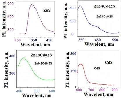
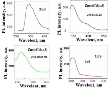
Figure 5 displays the PL spectra of the samples dispersed in ethanol. PL peaks are shifted to higher wavelength as Cd content increases.
The above results reveal that ZnS, CdS and ZnxCd1-xS nanoparticles are successfully obtained at room temperature and the compositions have been controlled. It is observed that by changing the ratio of ZnCl2, CdCl2 in the reactants the two phases Zn0.8Cd0.2S and Zn0.5Cd0.5S S are obtained. The control of the composition of ZnxCd1-xS nanoparticles may lead to the development of ideal materials for short wavelength diode laser applications.
1 I.A. Kariper, C. Gümüş, E. Güneri, F. Göde, Journal of Physics: Conference Series 326 (2011).
2 I.A. Kariper, E. Güneri, T. Özpozan, F. Göde, C. Gümüş 129 (2011) 183.
3 I.A. Kariper, C. Gümüş, E. Güneri, F. Göde, Chalcogenide Letters 12 (2012) 11.
4 Z.Qi.J. Deng, Y. Zhang, Q. Liao, Y. Huang, Nanotechnology 18(47) (2007) 475603.
5 I.O. Oladeji, L. Chow, Thin Solid Films 474(1) (2005) 77.
6 X. Wang, Z. Xie, H. Huang, Z. Liu, D. Chen, G. Shen, Journal of Materials Chemistry. 22(14) (2012) 6845.
7 Y. Liang, H. Liang, X. Xiao, S. Hark, Journal of Materials Chemistry. 2012;22(3):1199-1205.
8 C.S. Pathak, M.K. Mandal, V. Agarwala, Superlattices and Microstructures. 58 (2013) 135.
9 K. Nagamani, M.V. Reddy, Y. Lingappa, K.T. Ramakrishna, R.W. Miles, International J. of Optoelectronic Engineering 2 (2012) 1
M.A. Jafarov, S.A. Mamedova, E.F. Nasirov, Low-temperature technology to create photovoltaic cells solar energy, UNEC J. Eng. Appl. Sci 2(2) (2022) 18-22
Anyone you share the following link with will be able to read this content:
This article is licensed under the Creative Commons Attribution ( CC BY 4.0 ) License, which permits unrestricted use, distribution, and reproduction in any medium, provided the original author and source are credited.


I.A. Kariper, C. Gümüş, E. Güneri, F. Göde, Journal of Physics: Conference Series 326 (2011).
I.A. Kariper, E. Güneri, T. Özpozan, F. Göde, C. Gümüş 129 (2011) 183.
I.A. Kariper, C. Gümüş, E. Güneri, F. Göde, Chalcogenide Letters 12 (2012) 11.
Z.Qi.J. Deng, Y. Zhang, Q. Liao, Y. Huang, Nanotechnology 18(47) (2007) 475603.
I.O. Oladeji, L. Chow, Thin Solid Films 474(1) (2005) 77.
X. Wang, Z. Xie, H. Huang, Z. Liu, D. Chen, G. Shen, Journal of Materials Chemistry. 22(14) (2012) 6845.
Y. Liang, H. Liang, X. Xiao, S. Hark, Journal of Materials Chemistry. 2012;22(3):1199-1205.
C.S. Pathak, M.K. Mandal, V. Agarwala, Superlattices and Microstructures. 58 (2013) 135.
K. Nagamani, M.V. Reddy, Y. Lingappa, K.T. Ramakrishna, R.W. Miles, International J. of Optoelectronic Engineering 2 (2012) 1