UNEC Journal of Engineering and Applied Sciences Volume 1, No 1, pages 22-26 (2021) Cite this article, ![]() 2393
2393
The possibilities of creating contact structures based on single crystals of layered semiconductors n-InSe and p-GaSe in a much simpler way make them promising materials for the development of the physics of heterostructures and the creation of various functional elements of solid-state electronics. However, random macroscopic defects arising due to weak interlayer coupling in these semiconductors lead to scatter and instability of the main characteristics of heterostructures created on their basis. Since this disadvantage often comes to the fore during the operation of the corresponding elements, the establishment of ways to eliminate the scatter and instability of the parameters of p-GaSe/n-InSe heterostructures is of considerable scientific and practical interest.
Formulation of the problem
Early works [1, 2] reported the possibility of varying the influence of random macroscopic defects on generation – recombination processes and carrier drift in n-InSe and p-GaSe single crystals by doping them.
The aim of this work was to study the possibility of increasing the reproducibility and stability of the parameters of heterostructures [3] based on n-InSe and p-GaSe single crystals by doping them. For this, under various conditions, the effect of doping with erbium on the electrical and photoelectric properties of p-GaSe / n-InSe heterostructures has been experimentally investigated.
The objects of research were heterostructures created by planting on an optical contact [4] pure (not specially doped) and doped with erbium containing an introduced impurity (10-5<NEr<10-1 at.%) thin (with a thickness of 25£d£250 mm and transverse dimensions 2,0¸6,0х2,0¸6,0 mm2 in the direction perpendicular and along the plane (001) of the crystal, respectively) of the p-GaSe and n-InSe layers.
GaSe and InSe compounds are synthesized by the traditional method of joint fusion of their constituent components in evacuated quartz ampoules in a specially selected temperature regime. Alloying was carried out by introducing crushed metallic Er with a purity of 99.999% into the charge before the start of the synthesis process. The choice of Er as an impurity was related to the individual parameters and physicochemical properties of this chemical element [5]. Pure and doped single crystals of both semiconductors were grown by the Bridgman method.
Their structure, phase and elemental composition, as well as the state of the contacting surfaces of the contacting pairs were checked by structural analyzes using modern measuring devices and methods. It was found that the obtained unalloyed and Er-doped ingots of both semiconductors have a single-crystal structure, the diffraction patterns of InSe crystals are indexed in the rhombohedral system (g-polytope) and belong to the space group R3m C3v5 [6], and the diffractograms of GaSe crystals are in hexagonal polytyping (ε-) belong to the space group D3h1(P6) [7]. No other phases and free Er were found in the ingots obtained and on the surface of individual thin layers.
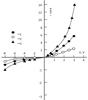
The studied heterostructures were created by uniform mechanical pressing of thin plates of contacting semiconductors in a special holder to each other. The current contacts were created by soldering in the open air without metal indium flux and were located so that during measurements the current and the light beam illuminating the structure under study were directed perpendicular to the (001) plane, i.e. perpendicular to the contact plane of the heterostructures under study. The dark static current-voltage (figure 1), spectral (figure 2) and light (figure 3) characteristics of the structures under study were measured experimentally in the temperature range 77<Т<350 К, at wavelengths (l) and intensities (Ф) of light 0.20<l<2.00 μm and Ф<5.102 LC, respectively
It was found that the investigated heterostructures have a diode character [3], and their forward direction corresponds to the case when the positive polarity of the applied voltage on the p-GaSe layer. The rectification coefficient (k) with voltage drops across the structure under study Ugp≈2¸3 V varies within ~ 6¸30 for different structures, in addition to thickness (d), it also depends on the value of the dark resistivity (ρТ0) at 77K and the content of the introduced impurity (NEr) contacting layers in the case of pure and doped samples, respectively. At Ug³0.5V, the exponential course of the direct branch of the CVC characteristic is replaced by a linear one.
At T=300 K, the cutoff voltage (U0) of the considered heterostructures [3] corresponds to the height of the potential barrier at the contact (~ 0.8¸1.1 V for various structures), and the residual resistance is ~ 5.104¸6.105 Ohm. With a change in the content of the introduced impurity (NEr), the diode character of the structures under study remains, however, the numerical values, as well as the stability and reproducibility of the current cutoff voltage, residual resistance, and rectification coefficient change. In particular, with an increase in NEr to 10-3 at.%, the residual resistance increases by an order of magnitude, then (at NEr>10-3 at.%) it decreases, at NEr³10-2 at.% it becomes even less than the initial one (which takes place in structures based on the lowest resistance undoped p-GaSe and n-InSe crystals). In this case, the stability and reproducibility of the electrical parameters of the heterostructures under study also change nonmonotonically (at first they deteriorate and then improve relative to the initial value).
Figure 1. CVC of p-GaSe<Er>/n-InSe<Er> structures for various N. NEr, at. %: 1-0; 2-10-3; 3-10-1. T = 150 K
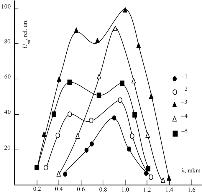
Figure 2. The photo-e.m.f. spectrum in p-GaSe<Er>/n-InSe<Er> structures. NEr, at.%: 1, 2 - 0; 3, 4 - 10-3; 5 - 10-1; T = 150 K; Ф=Фmax
2, 4 - when illuminated from the n-InSe<Er> side. 1, 3, 5 - when illuminated from the p-GaSe<Er> side
The photoelectric properties of the investigated heterostructures were studied in the photovoltaic mode [3] under illumination with light pulses with a repetition rate of 100÷150 Hz. It was found that in all the cases considered by us, the contacting GaSe component is charged negatively with respect to InSe, and the maximum value of the photovoltage (Uphv) is observed under illumination from the side of wide-gap p-GaSe. When illuminated from the side of a narrow-gap n-InSe, the character of the photosensitivity spectrum is completely determined by absorption in this semiconductor and turns out to be similar to the spectrum of an n-InSe photoresistor.
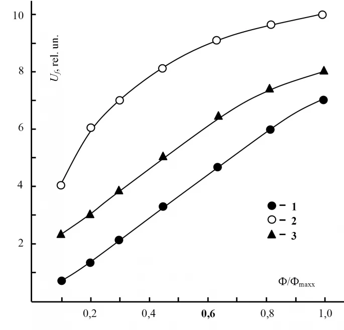
Figure 3. Light characteristic of p-GaSe<Er>/n-InSe<Er> heterostructures. NEr, at.%: 1 - 0; 2 - 10-3; 3 - 10-1
In this case, a discontinuity is observed only in the short-wavelength region (at l£0.50 mm) of the spectrum. Under illumination from the side of p-GaSe, two sections are observed in the photovoltage spectrum: the short-wavelength one corresponds to the absorption of light in p-GaSe, and the long-wavelength one - in n-InSe. Under optimal conditions, the open circuit voltage (Uс) and short circuit current (icc) [3] in the investigated heterostructures are ~ 0.35 V and ~ 45 μA/cm2, respectively. In the region of low temperatures for both directions of illumination, the value of Uphv and the width of its spectrum increase with an increase in NEr to 10-3 at.%, and under illumination from the side of the p-GaSe component it covers the wavelength range of ~ 0.25÷1.45 μm, and the stability and reproducibility of their parameters deteriorate markedly. With a further increase in NEr to 10-1 at.%, the value of Uphv and the width of its spectrum, decreasing, approach the corresponding heterostructure based on pure crystals with the smallest ρТ0. However, in this case, the maximum stability and reproducibility of the parameters and characteristics of the heterostructures is observed. The degrees of stability and reproducibility of the parameters of heterostructures were checked by 10÷20 times tests of the same sample, and their reproducibility was tested by comparing 10÷15 different samples.
With a decrease in the thickness of the contacting pairs, in addition to improving the electrical and photoelectric parameters, the flexibility of the investigated heterostructures also increases, which makes them extremely operational.
A static analysis of the experimental results obtained shows that the tunneling mechanism of current passage dominates in the heterostructures under study in the presence of local centers in the band gap of contacting semiconductors. The unequal effect of light upon illumination of the investigated photocells from the side of p-GaSe and n-InSe is associated with the "window effect" [3], and a sharp drop in the photovoltage value from the side of short wavelengths - with a small value of the diffusion length of nonequilibrium charge carriers in both contacting semiconductors in direction perpendicular to the natural layers of crystals in comparison with the thickness of individual layers [8].
The scatter of characteristics and parameters of different heterostructures and their dependence on NEr are associated with the presence of random macroscopic defects (RMD) in p-GaSe and n-InSe crystals [9], which are caused by the weakness of the interlayer bond and differ significantly from sample to sample. In pure crystals, with an increase in ρТ0, the number and size of the RMD increases. Accordingly, the role of the fluctuations of the electron potential created by them in conductivity and photoelectric phenomena also increases. In doped crystals with a very low solubility in semiconductors, erbium atoms, accumulating on random macroscopic defects, increase their size. At NEr<10-4 at.% and NEr<10-3 at.% for p-GaSe and n-InSe crystals, respectively, the space charge regions (SCR) of neighboring RMD do not yet overlap and the random potential compared with the existing in pure crystals is great. Therefore, with an increase in NEr, the associated features of photoelectric phenomena increase. With a further increase in NEr, the SCR of neighboring RMD begin to overlap. As a result, the random potential and its influence on the generation-reconbination and drift processes decreases [10, 11]. In addition, doping with erbium, healing the defectiveness of the crystal, increases the reproducibility and stability of the parameters and characteristics of heterostructures created on their basis.
Thus, we can conclude that flexible heterostructures with highly reproducible and stable parameters and characteristics can be created on the basis of erbium-doped p-GaSe and n-InSe single crystals. The most effective for this purpose is alloying with NEr ≈ 10-1 at.%.
1 A.S. Abdinov, R.F. Babaeva, M.A. Dzhafarov, R.M. RzaeV, N.A. Ragimova, Inorganic materials 35(4) (1999) 325-327.
2 A.Sh. Abdinov, R.F. Babaeva, N.A. Ragimova, R.M. Rzaev, S.I. Amirova, Inorganic Materials 50(4) (2014) 334–338.
3 B.L. Sharma, R.K. Purokhit. Semiconductor heterojunctions. M. Soviet radio (1979) 228 p.
4 V.L. Bakumenko, Z.D. Kovalyuk, L.N. Kurbatov, V.G.Tagayev, V.F. Chishko, Semiconductors 6 (1980) 1115-1119.
5 Ya.A. Ugai. General inorganic chemistry. M. "Higher school", (in Russian) (1997) 527 p.
6 A. Likforman, D. Carré, J.Etienne , B. Bachet, Acta Cryst. 31 (1975) 1252-1254.
7 A. Kuhn, A. Chevy, R. Chevalier, Рhys. stat. sol. (a) 31 (1975) 469-475.
8 Z.S. Medvedeva, Chalcogenides of elements III B of the subgroup of the periodic system. M.: Nauka, (in Russian) (1968) 216 p.
9 A.Ya. Shik, Zh. Eksp. Teor. Fiz. 15 (1972) 408–410.
10 B.I. Shklovskii, A.L. Efros, Elektronnye svoistva legirovannykh poluprovodnikov (Electronic Properties of Doped Semiconductors), Moscow: Nauka, ( 1979) 416 p.
11 A.Sh. Abdinov, R.F. Babayeva, Russian Physics Journal 61(9) (2019) 1667-1673.
R.F. Babayeva, A.Sh. Abdinov, N.A. Ragimova, S.I. Amirova, E.A. Rasulov, The possibility of increasing the reproductivity and stability of the characteristics of n-InSe/p-GaSe heterostructures, UNEC J. Eng, Appl. Sci. 1(1) (2021) 22-26
Anyone you share the following link with will be able to read this content:
This article is licensed under the Creative Commons Attribution ( CC BY 4.0 ) License, which permits unrestricted use, distribution, and reproduction in any medium, provided the original author and source are credited.


A.S. Abdinov, R.F. Babaeva, M.A. Dzhafarov, R.M. RzaeV, N.A. Ragimova, Inorganic materials 35(4) (1999) 325-327.
A.Sh. Abdinov, R.F. Babaeva, N.A. Ragimova, R.M. Rzaev, S.I. Amirova, Inorganic Materials 50(4) (2014) 334–338.
B.L. Sharma, R.K. Purokhit. Semiconductor heterojunctions. M. Soviet radio (1979) 228 p.
V.L. Bakumenko, Z.D. Kovalyuk, L.N. Kurbatov, V.G.Tagayev, V.F. Chishko, Semiconductors 6 (1980) 1115-1119.
Ya.A. Ugai. General inorganic chemistry. M. "Higher school", (in Russian) (1997) 527 p.
A. Likforman, D. Carré, J.Etienne , B. Bachet, Acta Cryst. 31 (1975) 1252-1254.
A. Kuhn, A. Chevy, R. Chevalier, Рhys. stat. sol. (a) 31 (1975) 469-475.
Z.S. Medvedeva, Chalcogenides of elements III B of the subgroup of the periodic system. M.: Nauka, (in Russian) (1968) 216 p.
A.Ya. Shik, Zh. Eksp. Teor. Fiz. 15 (1972) 408–410.
B.I. Shklovskii, A.L. Efros, Elektronnye svoistva legirovannykh poluprovodnikov (Electronic Properties of Doped Semiconductors), Moscow: Nauka, ( 1979) 416 p.
A.Sh. Abdinov, R.F. Babayeva, Russian Physics Journal 61(9) (2019) 1667-1673.